
Formation method of semiconductor structure
A semiconductor and gate structure technology, applied in the field of semiconductor structure formation, can solve the problem that the electrical performance of the semiconductor structure needs to be improved, etc.
Patent Information
- Authority / Receiving Office
- CN · China
- Patent Type
- Patents(China)
- Current Assignee / Owner
- Publication Date
- 2016-09-28
Smart Images
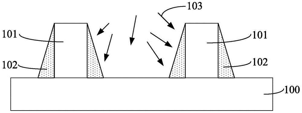
Figure 1 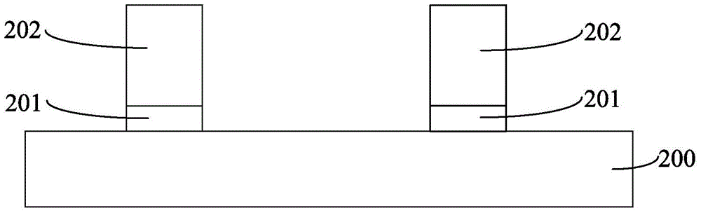
Figure 2 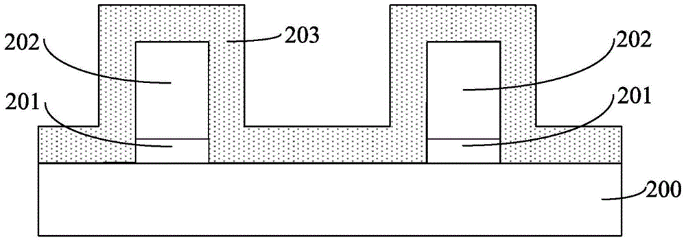
Figure 3
Abstract
Description
technical field
[0001] The invention relates to the technology in the field of semiconductor manufacturing, in particular to a method for forming a semiconductor structure. Background technique
[0002] With the continuous increase of the integration level of semiconductor devices, the critical dimensions of semiconductor devices are continuously reduced, and many problems have appeared correspondingly, such as the corresponding increase in surface resistance and contact resistance of the drain, source and gate structures of semiconductor devices, resulting in the decrease of semiconductor devices. The response speed is reduced and the signal is delayed. Therefore, an interconnection structure with low resistivity becomes a key element in the manufacture of highly integrated semiconductor devices.
[0003] In order to reduce the contact resistance of the drain-source and gate structures of semiconductor devices, the process method of metal silicide is introduced. The metal ...
Examples
Embodiment Construction
[0023] It can be seen from the background art that the electrical performance of the semiconductor structure formed in the prior art still needs to be improved.
[0024] It has been found through research that during the formation of the semiconductor structure, after forming the source region, the drain region and the gate structure, in order to reduce the contact resistance of the semiconductor structure, metal silicide is usually formed on the surface of the source region, the drain region and the gate structure, in order to To improve the quality of the formed metal silicide and reduce the resistivity of the metal silicide material, it is required that the surface of the source region, the drain region and the gate structure have a high degree of cleanliness. For this reason, before forming the metal silicide, the surface of the source region, the drain region and the gate structure are cleaned to remove impurities on the surface of the source region, the drain region and t...