
Anti-radiation D latch based on dual interlocking structure
A latch, double interlock technology, applied in the directions of radiation tolerance enhancement, reliability improvement modification, delay compensation, etc., can solve the problem of poor resistance to double-node flipping, failure to achieve double-node flipping fault tolerance, long delay time, etc. question
Patent Information
- Authority / Receiving Office
- CN · China
- Current Assignee / Owner
- Publication Date
- 2019-04-05
- Estimated Expiration
- Not applicable · inactive patent
Smart Images
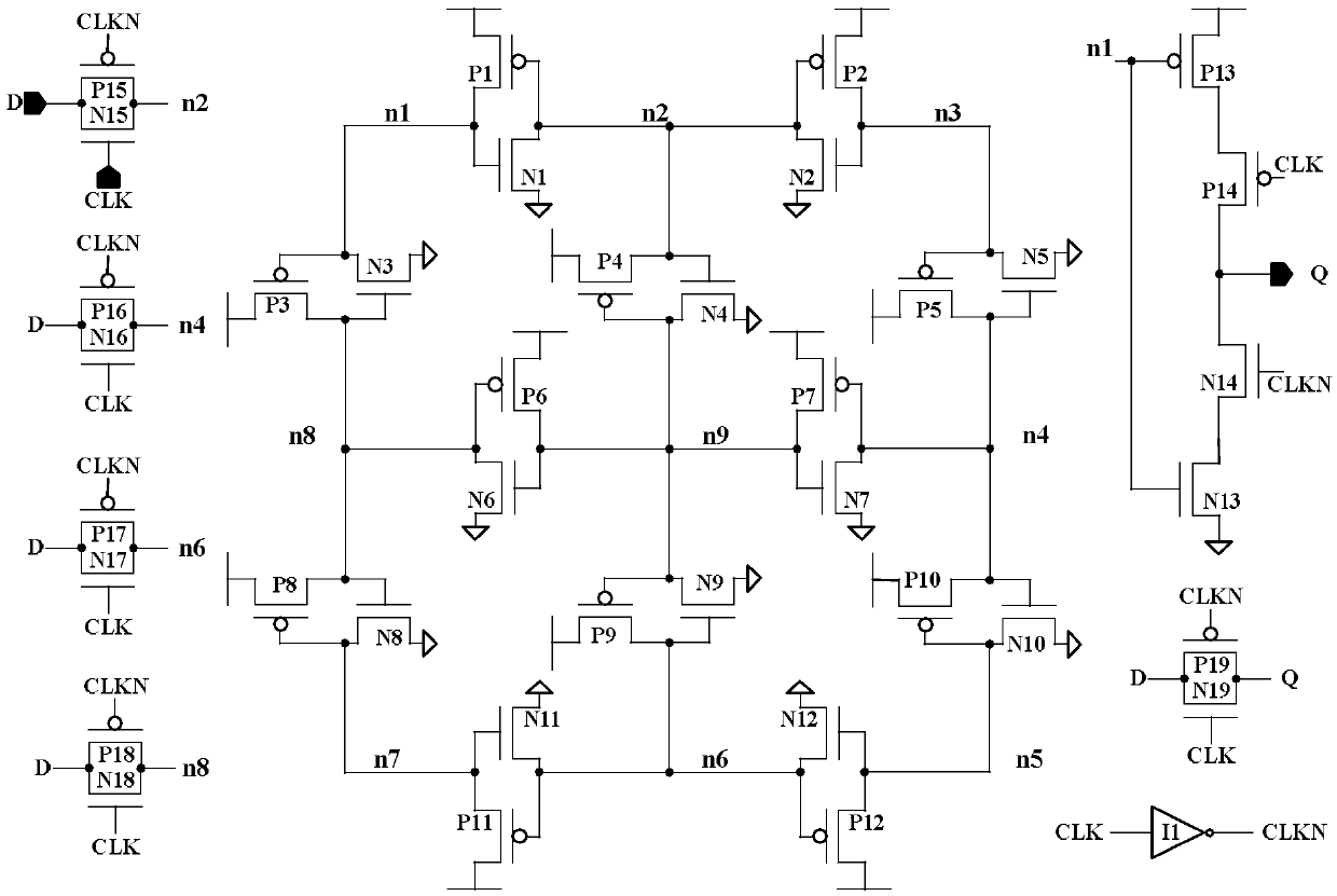
Figure 1 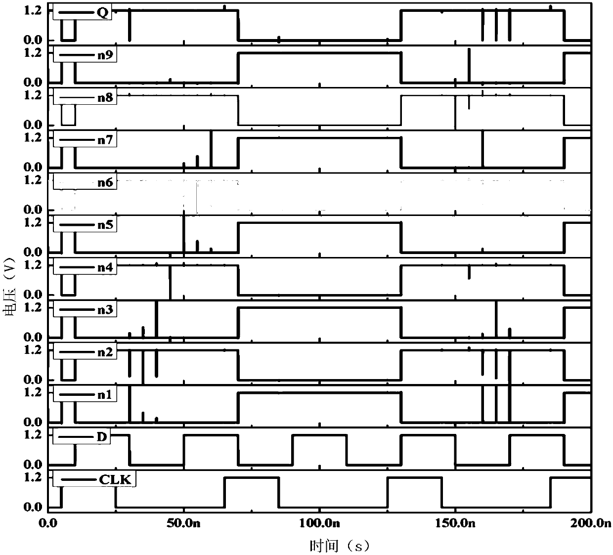
Figure 2
Abstract
Description
technical field
[0001] The invention belongs to the field of anti-radiation reinforcement in integrated circuit reliability. Background technique
[0002] In aerospace and high-radiation applications on the ground, the D latch needs to be hardened against radiation, mainly to prevent the stored data from being changed by external radiation particles. The traditional anti-radiation D latch is generally reinforced by triple-mode redundancy. The disadvantages are that it requires more hardware (up to 102 transistors), high power consumption, long delay time, and although it can achieve anti-double node flipping, However, the ability to resist double-node flipping is poor, and it is even impossible to achieve fault tolerance to double-node flipping. Therefore, the above problems need to be solved urgently. Contents of the invention
[0003] The present invention aims to solve the problem that the traditional anti-radiation D latch needs more hardware, high power consumption,...
Examples
Embodiment Construction
[0086] The following will clearly and completely describe the technical solutions in the embodiments of the present invention with reference to the accompanying drawings in the embodiments of the present invention. Obviously, the described embodiments are only some, not all, embodiments of the present invention. Based on the embodiments of the present invention, all other embodiments obtained by persons of ordinary skill in the art without making creative efforts belong to the protection scope of the present invention.
[0087] It should be noted that, in the case of no conflict, the embodiments of the present invention and the features in the embodiments can be combined with each other.
[0088] The present invention will be further described below in conjunction with the accompanying drawings and specific embodiments, but not as a limitation of the present invention.
[0089] see figure 1 Describe this embodiment mode, the anti-irradiation D latch based on the double interl...