
GMR magnetic nanometer multilayer film used for magneto-dependent sensor
A magnetic sensor and magnetic nanotechnology, which is applied in the field of precision measurement and magnetic materials, can solve the problems of low giant magnetoresistance ratio, poor linear range adjustability, and low magnetic field sensitivity of magnetic sensitive sensors, so as to improve magnetic field sensitivity and improve roughness Degree, the effect of increasing the giant magnetoresistance ratio
Patent Information
- Authority / Receiving Office
- CN · China
- Current Assignee / Owner
- Publication Date
- 2015-09-09
- Estimated Expiration
- Not applicable · inactive patent
Smart Images
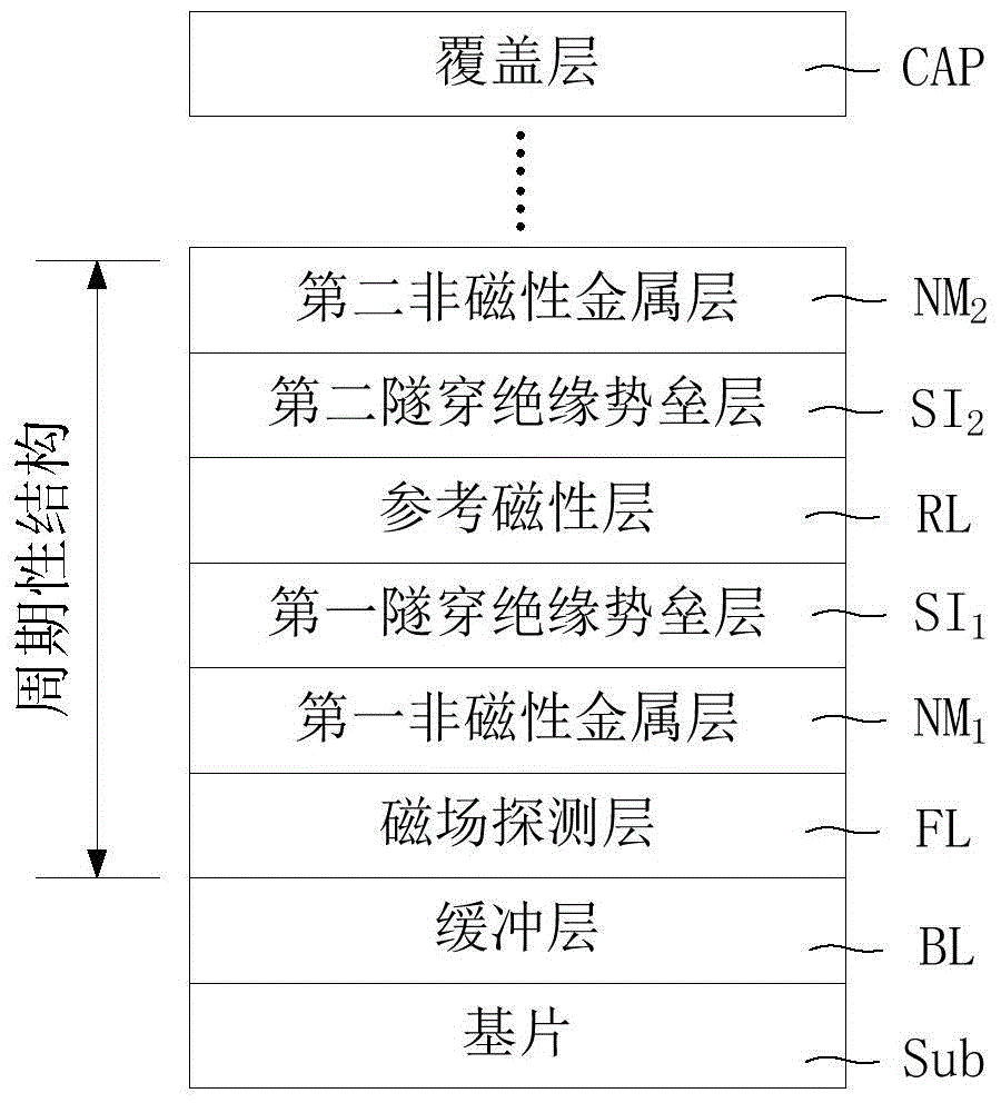
Figure 1 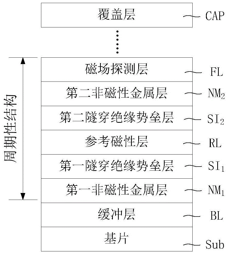
Figure 2 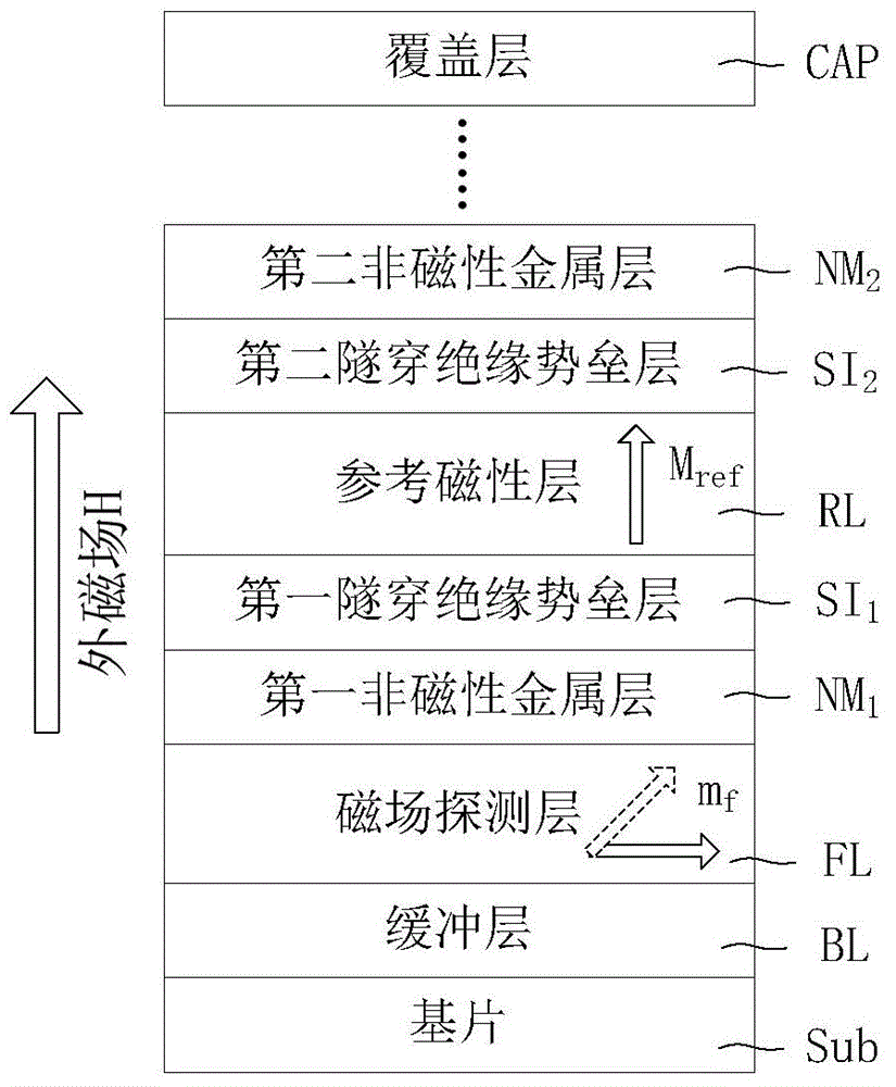
Figure 3
Abstract
Description
technical field
[0001] The invention belongs to the technical field of precision measurement and magnetic materials, and relates to a magnetic sensor, in particular to a GMR magnetic nano-multilayer film used for a magnetic sensor. Background technique
[0002] Magnetic sensors are widely used in industrial fields such as current detection, angle measurement, biosensing, data reading, building monitoring, and non-destructive detection. Early magnetosensitive sensors were mainly based on semiconductor materials with Hall effect and magnetic materials with magnetic anisotropy magnetoresistance (AMR) effect. However, the magnetic sensor based on these two types of materials has low magnetic field sensitivity, narrow linear range, and low applicable temperature.
[0003] With the in-depth study of magnetic materials and the development of spintronics, magneto-sensitive sensors based on the Giant Magneto Resistive (GMR) effect and the tunneling magnetoresistance effect have the ...
Examples
Embodiment 1
[0046] 1) Using Si-SiO with a thickness of 1mm 2 The substrate is used as the substrate Sub, and a buffer layer BL is deposited on the surface of the substrate Sub by magnetron sputtering. The buffer layer BL includes stacked Ta layer and Au layer, and the thicknesses of the Ta layer and the Au layer are 5nm and 3nm respectively. In magnetron sputtering, the vacuum is preferably better than 6×10 -5 Pa.
[0047] 2) Deposit Ni on the surface of the buffer layer BL by magnetron sputtering technology 80 Fe 20 The material forms the magnetic field detection layer FL. In magnetron sputtering, the vacuum is preferably better than 6×10 -5 Pa, the deposition rate is about 0.1nm / s.
[0048] 3) Using magnetron sputtering technology to deposit Au on the surface of the magnetic field detection layer FL to form the first non-magnetic metal layer NM 1 . In magnetron sputtering, the vacuum is preferably better than 6×10 -5 Pa, the deposition rate is about 0.2nm / s.
[0049] 4) Using m...
Embodiment 2
[0060] The GMR magnetic nano-multilayer film was prepared by the same manufacturing method as in Example 1, the difference lies in the structure and thickness of the GMR magnetic nano-multi-layer film. The structure of the magnetic nano multilayer film prepared by embodiment 2 is: Sub / BL / [FL / NM 1 / SI / RL / NM 2 ] 10 / CAP. The specific composition and thickness of each layer of the GMR magnetic nano-multilayer film are shown in Attached Table 2.
[0061] Schedule 2
[0062] Substrate
Embodiment 3
[0064] The GMR magnetic nano-multilayer film was prepared by the same manufacturing method as in Example 1, the difference lies in the structure and thickness of the GMR magnetic nano-multi-layer film. The structure of the magnetic nano multilayer film prepared by embodiment 3 is: Sub / BL / [FL / NM 1 / RL / SI / NM 2 ] 5 / CAP. The specific composition and thickness of each layer of the GMR magnetic nano-multilayer film are shown in Attached Table 3.
[0065] Schedule 3
[0066] Substrate