
Minkowski-based microstrip patch antenna and manufacturing method thereof
A microstrip patch antenna and microstrip patch technology, which are applied in the field of wireless communication, can solve the problems of antenna size limitation, large antenna size, and difficulty in conformality, and achieve the effect of overcoming large size, easy integration, and easy conformality.
Patent Information
- Authority / Receiving Office
- CN · China
- Current Assignee / Owner
- Publication Date
- 2017-06-23
- Estimated Expiration
- Not applicable · inactive patent
Smart Images
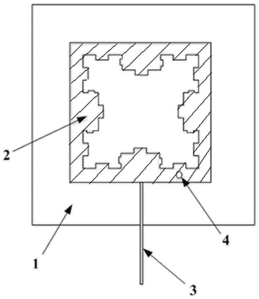
Figure 1 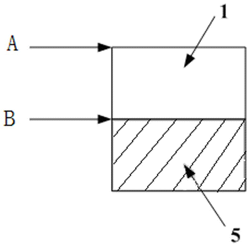
Figure 2 
Figure 3
Abstract
Description
technical field
[0001] The invention belongs to the field of wireless communication, and in particular relates to a Minkowski-based microstrip patch antenna and a manufacturing method thereof. Background technique
[0002] Radio Frequency Identification (RFID) technology can be traced back to the radio frequency identification system proposed by the British Air Force during World War II. During the Battle of Britain, the fighter planes of the British and German air forces were very similar in appearance, and they could not be accurately identified with the naked eye during high-speed flight. The British Air Force has installed a response device on its own fighter plane, which transmits the pre-programmed pulse code through the interrogation device on the ground. If it is its own fighter plane, the response device on the fighter plane will send the agreed pulse code Reflected to the land station; if the fighter emits a wrong code or does not respond, it is judged as an enemy...
Examples
Embodiment Construction
[0028] The present invention will be further described below in conjunction with drawings and embodiments.
[0029] like figure 1 , 2 As shown, a microstrip patch based on the secondary Minkowski fractal structure is composed of a dielectric plate 1, a radiation unit 2, a feed unit 3, a ground via 4 and a ground unit 5, and the dielectric plate has a first surface A and the second surface B corresponding thereto; the radiation unit 2 is arranged on the first surface A of the dielectric board 1; the feed unit 3 is connected to the radiation unit 2 and is also arranged on the first surface A of the dielectric board 1 Above; the ground via hole 4 passes through the radiation unit 2 and the dielectric board 1 when punching, so that the radiation unit 2 communicates with the ground unit 5 to form a short circuit; the ground unit 5 is arranged on the second surface B of the dielectric board 1, and The dielectric plate 1 may not be completely covered. However, the high-frequency e...