
Fabrication method of vertical double diffusion metal oxide semiconductor (VDMOS) device
A manufacturing method and device technology, applied in semiconductor/solid-state device manufacturing, semiconductor devices, electrical components, etc., can solve the problems of complex manufacturing process and inability to eliminate the influence of feedback capacitance well
Patent Information
- Authority / Receiving Office
- CN · China
- Current Assignee / Owner
- Publication Date
- 2017-09-15
- Estimated Expiration
- Not applicable · inactive patent
Smart Images
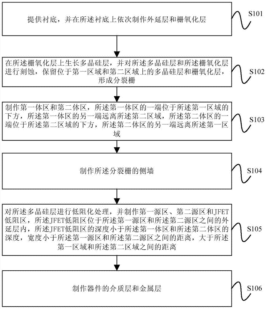
Figure 1 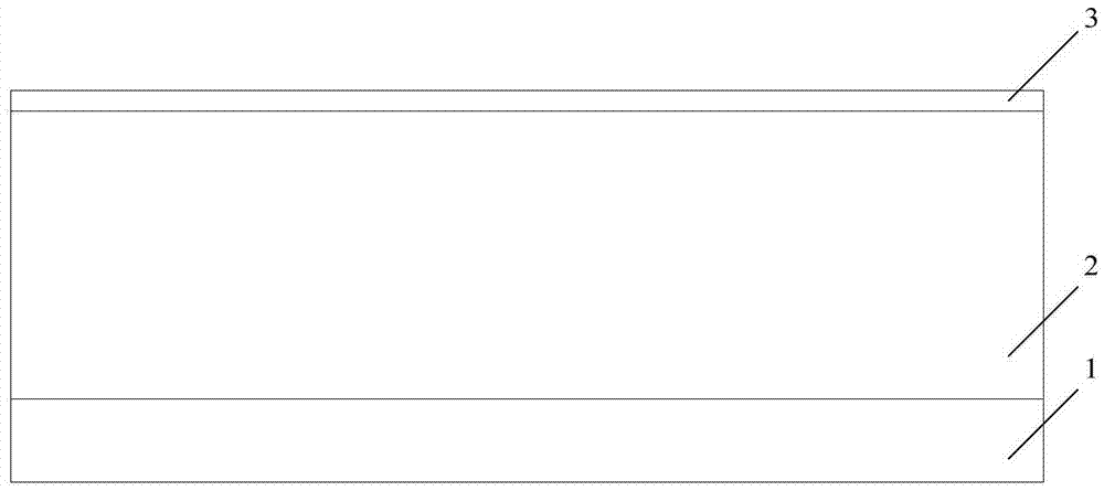
Figure 2 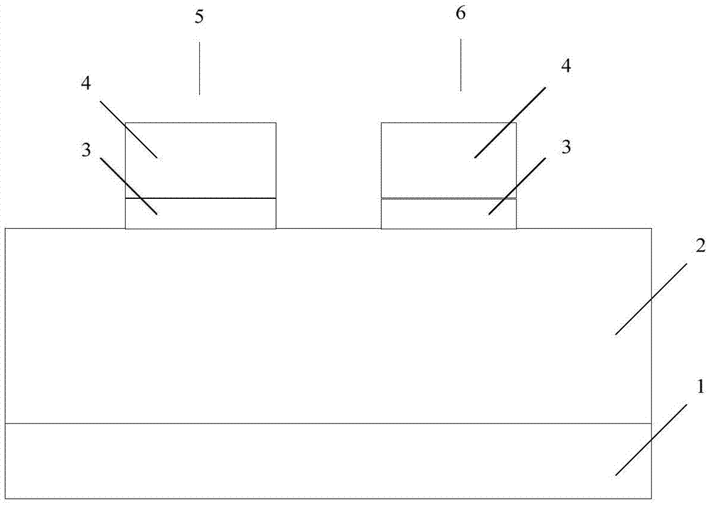
Figure 3
Abstract
Description
technical field
[0001] Embodiments of the present invention relate to the technical field of semiconductor device manufacturing, and in particular, to a method for manufacturing a VDMOS device. Background technique
[0002] Vertical double-diffused field-effect transistor (VDMOS) is one of the commonly used power transistors at present, and the feedback capacitance has always been the main factor affecting its performance.
[0003] The method of reducing the feedback capacitance in the prior art mainly starts from reducing the oxide capacitance between the gate and the drain, such as increasing the thickness of the gate oxide layer as a whole or locally increasing the thickness of the gate oxide layer. However, in the prior art, no matter whether the method of increasing the thickness of the gate oxide layer as a whole or locally increases the thickness of the gate oxide layer, it cannot well eliminate the influence of the feedback capacitor on VDMOS, and the manufacturing p...
Examples
Embodiment Construction
[0027] The following will clearly and completely describe the technical solutions in the embodiments of the present invention with reference to the accompanying drawings in the embodiments of the present invention. Obviously, the described embodiments are only some, not all, embodiments of the present invention. Based on the embodiments of the present invention, all other embodiments obtained by persons of ordinary skill in the art without making creative efforts belong to the protection scope of the present invention.
[0028] The terms "comprising" and "having" and any variations thereof in the description and claims of the present invention are intended to cover a non-exclusive inclusion, for example, a process comprising a series of steps or a device of structure need not be limited to the expressly listed Instead, those structures or steps may include other steps or structures not expressly listed or inherent to the process or device.
[0029] figure 1 A schematic flow c...