
Semiconductor device
A semiconductor, conductive type technology, applied in the fields of semiconductor devices, semiconductor/solid-state device manufacturing, electrical components, etc., can solve the problems of reduced switching speed, large feedback capacitance, etc., to achieve the effect of reducing feedback capacitance
Patent Information
- Authority / Receiving Office
- CN · China
- Current Assignee / Owner
- Publication Date
- 2018-01-30
- Estimated Expiration
- Not applicable · inactive patent
Smart Images
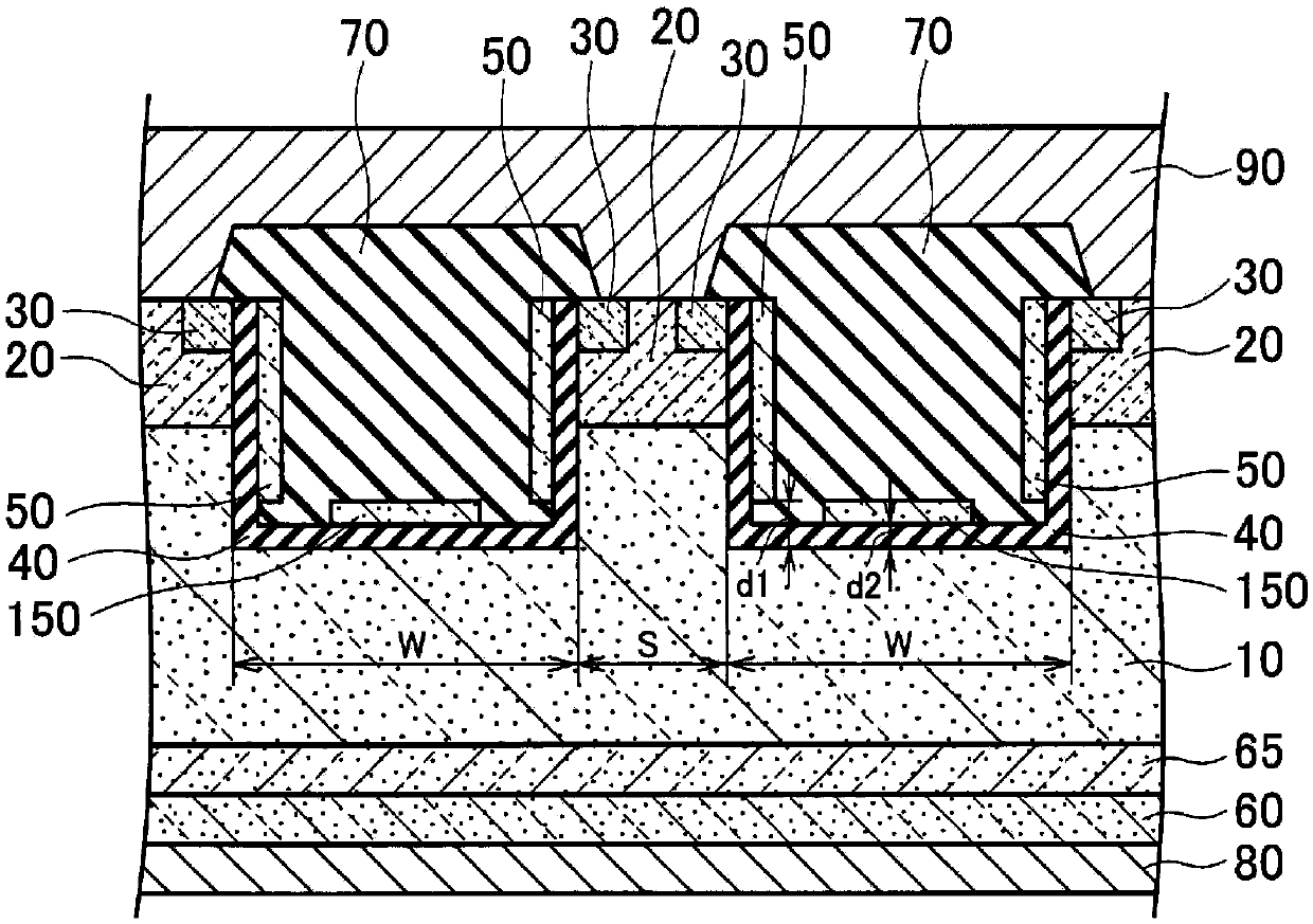
Figure 1 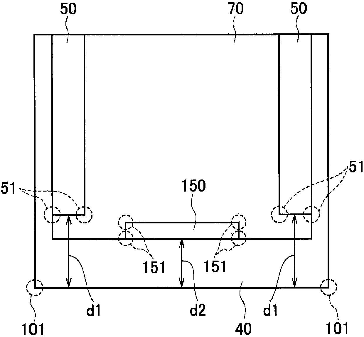
Figure 2 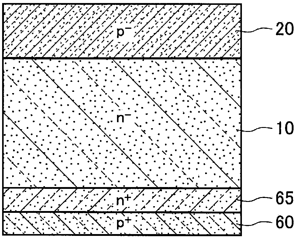
Figure 3
Abstract
Description
technical field
[0001] The present invention relates to trench gate semiconductor devices. Background technique
[0002] A power MOSFET, an insulated gate bipolar transistor (IGBT), or the like is used as a switching element (power semiconductor element) that performs a switching operation of a large current. These switching elements employ a trench-type gate electrode structure (trench gate type), in which a gate insulating film and a gate electrode are formed in a groove (trench) formed in a semiconductor substrate. However, in trench gate semiconductor devices, the capacitance between the gate electrode and the drain region (gate-drain capacitance), the capacitance between the gate electrode and the collector region (gate-collector capacitance) etc. The feedback capacitance is larger. Therefore, the switching speed decreases, causing a problem in high-frequency operation.
[0003] Various methods for reducing the feedback capacitance are being investigated. For exampl...
Examples
other Embodiment approach
[0094] As mentioned above, although this invention was described using embodiment, it should not be understood that the description and drawing which make a part of this indication limit this invention. It is obvious that various alternative embodiments, examples, and applied techniques can be conceived by those skilled in the art from the present disclosure.
[0095] The above shows an example where the semiconductor device is an IGBT. However, the semiconductor device may also be a switching element of another trench gate type structure. Figure 14 An example in which the semiconductor device is a trench gate MOSFET is shown. Figure 14 The illustrated semiconductor device is a MOSFET having a structure in which an n-type drain region 160 is disposed on the lower surface of the drift region 10 . A drain electrode 180 electrically connected to the drain region 160 is disposed on the lower surface of the drain region 160 .
[0096] even if Figure 14 In the MOSFET semicond...