
A Diamond Field-Effect Transistor with Air-Bridge-Like Source-Field Plate Structure
A field effect transistor and source field plate technology, applied in the field of diamond field effect transistors, can solve the problems of reducing the operating frequency, power gain, etc., and achieves improving the power gain and operating frequency, increasing the breakdown voltage, and reducing the gate-drain feedback capacitance. Effect
Patent Information
- Authority / Receiving Office
- CN · China
- Patent Type
- Patents(China)
- Current Assignee / Owner
- Publication Date
- 2022-03-22
Smart Images
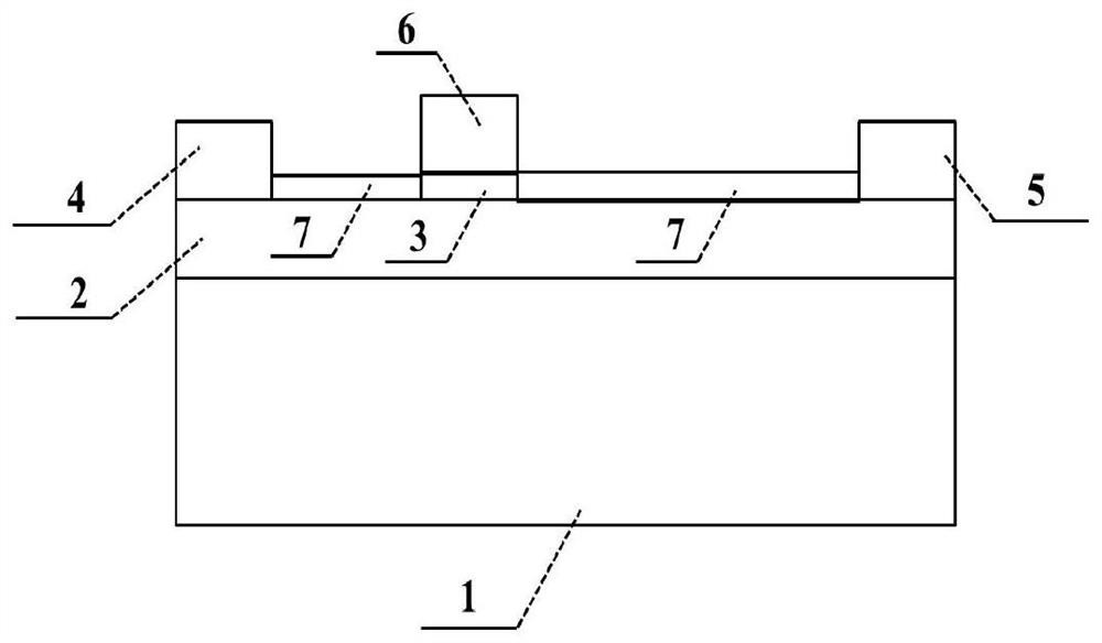
Figure 1 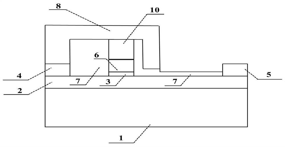
Figure 2 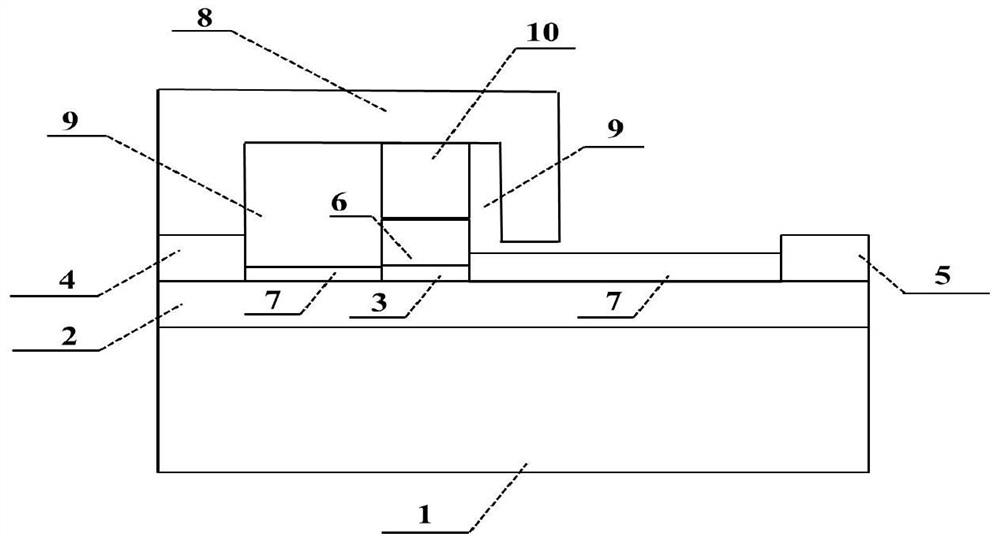
Figure 3
Abstract
Description
technical field
[0001] The invention relates to the field of diamond field effect transistors, in particular to a diamond field effect transistor with an air bridge-like source field plate structure. Background technique
[0002] In terms of material properties, the third-generation semiconductor gallium nitride (GaN) has the advantages of large band gap, high critical breakdown electric field, high electron saturation velocity, and strong radiation resistance. Therefore, gallium nitride high electron mobility transistors (GaN HEMT) has strong ability of high frequency, pressure resistance, high temperature resistance and harsh environment. However, its thermal conductivity is still very low compared with diamond, and there are serious traps, so there is current collapse when outputting high power density, which seriously restricts the output capability of high power density. Due to its high breakdown voltage, high power density, high electron mobility, and high thermal con...
Examples
Embodiment
[0034] use image 3 Shown is a diamond field effect transistor with an air bridge type source field plate structure. The substrate layer 1 is crystal-oriented single-crystal diamond with a thickness of 1.9 μm; the epitaxial layer 2 is crystal-oriented single-crystal diamond with a thickness of 100 nm, a gate-source distance of 0.2 μm, a gate-drain distance of 1 μm, and a gate length of 0.2 μm. , the passivation layer 7, the gate dielectric layer 3 and the support layer 10 of the source field plate 8 on the gate electrode are all aluminum oxide, but the thickness of the passivation layer 7 in the gate source region and the passivation layer 7 in the gate drain region are different, respectively The thicknesses of the gate dielectric layer 3 and the support layer 10 of the source field plate on the gate electrode are 10nm and 320nm respectively. The distance between the bottom of the source field plate 8 of the gate and drain region and the passivation layer 7 is 10 nm, with an...