
A titanium nitride atomic layer deposition device and its deposition method
A technology of atomic layer deposition and titanium nitride, which is applied in the direction of coating, gaseous chemical plating, metal material coating process, etc., can solve the problems of polluting the substrate surface, not being effective, and having no heating function, so as to avoid gas Effects of handling system settings, reducing undesired reactions, and reducing particle generation
Patent Information
- Authority / Receiving Office
- CN · China
- Patent Type
- Patents(China)
- Current Assignee / Owner
- Publication Date
- 2020-02-07
Smart Images
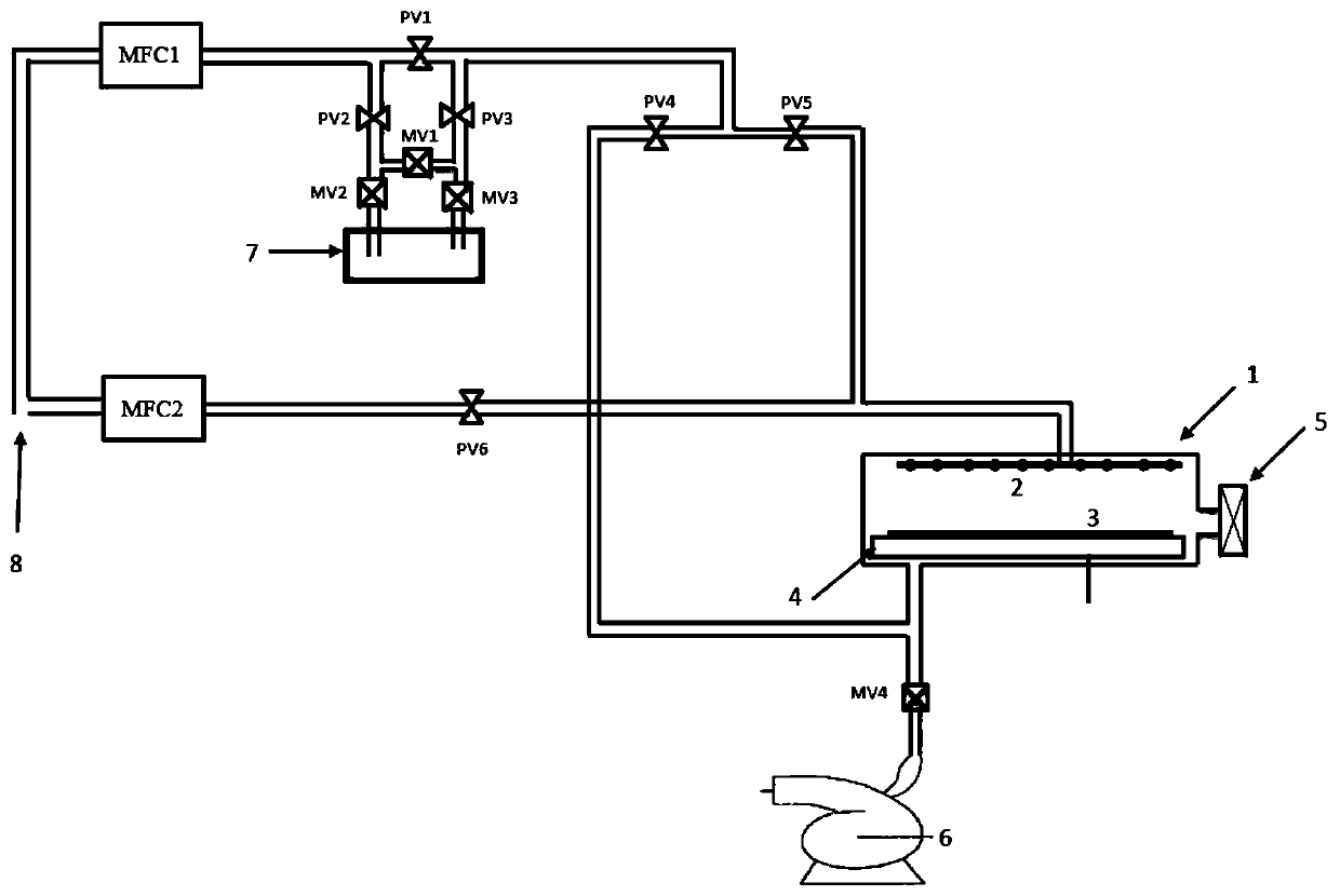
Figure 1 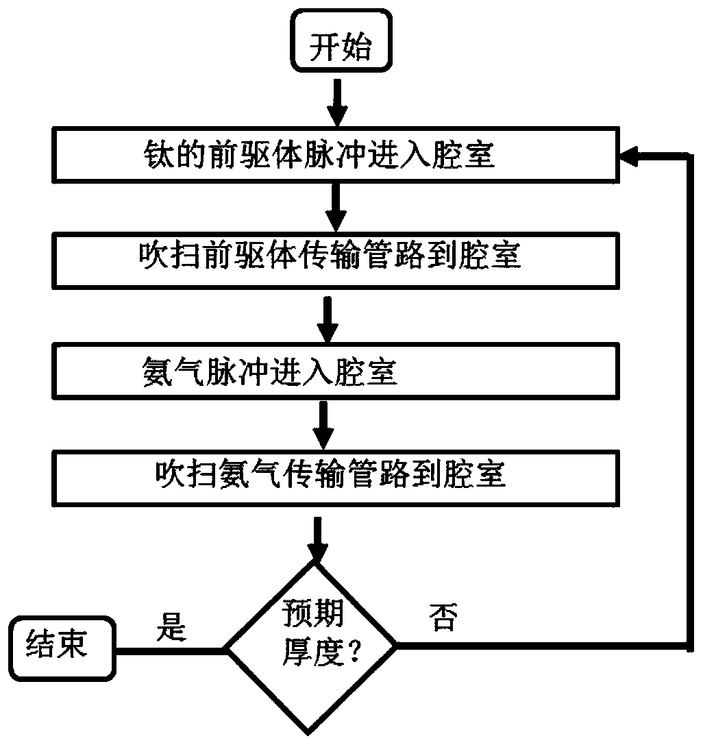
Figure 2 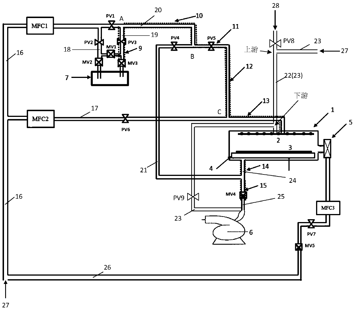
Figure 3
Abstract
Description
technical field
[0001] The invention relates to the technical field of semiconductor processing, and more specifically, to a titanium nitride atomic layer deposition device and a deposition method thereof. Background technique
[0002] Titanium nitride (TiN) is used as a coating for cutting tools because of its high hardness, high melting point, and good thermal and chemical stability. Moreover, titanium nitride has become a multi-purpose material in the IC field due to its good electrical conductivity, good thermal stability and mechanical properties of the film. Such as applied to Cu diffusion barrier (copper diffusion barrier), CMOS diodes and gate electrodes of DRAM capacitor components, etc.
[0003] PVD and CVD methods are the main methods for depositing TiN thin films. However, studies have shown that compared with TiN films deposited by PVD and CVD methods, TiN films deposited by atomic layer deposition (ALD) have better step coverage. Especially with the reductio...
Examples
Embodiment Construction
[0064] The specific embodiment of the present invention will be further described in detail below in conjunction with the accompanying drawings.
[0065] It should be noted that, in the following specific embodiments, when describing the embodiments of the present invention in detail, in order to clearly show the structure of the present invention for the convenience of description, the structures in the drawings are not drawn according to the general scale, and are drawn Partial magnification, deformation and simplification are included, therefore, it should be avoided to be interpreted as a limitation of the present invention.
[0066] In the following specific embodiments of the present invention, please refer to image 3 , image 3 It is a schematic structural diagram of a titanium nitride atomic layer deposition device according to a preferred embodiment of the present invention. Such as image 3 As shown, a titanium nitride atomic layer deposition device of the presen...