
Thermoelectric coupling modeling method of power semiconductor chip cell
A power semiconductor and thermoelectric coupling technology, applied in CAD numerical modeling, electrical digital data processing, instruments, etc., can solve the problem of accurate characterization of chip electrical characteristics, prediction of chip electrical temperature field accuracy disadvantages, and complex application environment of power semiconductor chips And other issues
Patent Information
- Authority / Receiving Office
- CN · China
- Patent Type
- Applications(China)
- Current Assignee / Owner
- Publication Date
- 2021-04-23
Smart Images
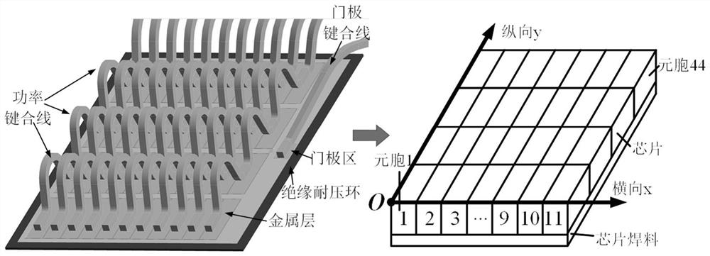
Figure 1 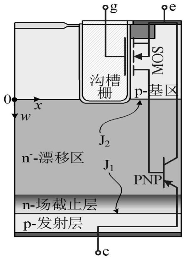
Figure 2 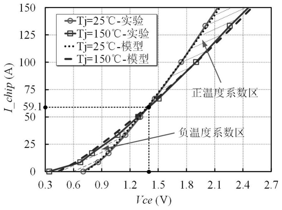
Figure 3
Abstract
Description
technical field
[0001] The invention belongs to the field of power electronic devices, and in particular relates to a thermoelectric coupling modeling method of power semiconductor chip cells. Background technique
[0002] Power modules are widely used in new energy vehicle powertrain systems. The trend of high power density and high integration intensifies the temperature gradient on the chip surface, and the electrical parameters of the cells have a temperature change effect, which leads to the uneven distribution of current density on the chip. Due to the over-current operation of semiconductor chips under extreme working conditions such as low-speed high-torque, heavy-duty stator stalls, and acceleration during start-up, the uneven distribution of cell current is more serious, and the formation mechanism of the on-chip temperature field is still unclear. to hidden dangers. Therefore, it is particularly urgent to model and analyze the electrical temperature field on the...
Examples
Embodiment Construction
[0056] In order to explain the present invention in more detail, the present invention will be further described in detail below in conjunction with the accompanying drawings, taking the SEMiKron power semiconductor module SEMiX603GB12E4p as an example.
[0057] The thermoelectric coupling modeling method of the power semiconductor chip cell proposed by the present invention, the specific steps include:
[0058] S1. Based on the chip metal layer and bonding wire layout characteristics, the power semiconductor chip is divided into a multi-cell structure;
[0059] S2. Extract chip lumped parameters, and use the least squares algorithm to establish a voltage-current-temperature three-dimensional model of the power semiconductor chip;
[0060] S3. According to the characteristics of the multi-cell parallel circuit, the chip lumped parameters are converted into cell distribution parameters, and the voltage-current-temperature three-dimensional model of the power semiconductor cell ...