
Method for manufacture prism
A manufacturing method and prism technology, which are applied to prisms, manufacturing tools, and machine tools suitable for grinding workpiece planes, etc., can solve the problems of inclined sidewall errors, cutting errors, and cannot guarantee high-precision angular accuracy, and achieve high angular accuracy. Effect
Patent Information
- Authority / Receiving Office
- CN · China
- Current Assignee / Owner
- Publication Date
- 2006-12-06
- Estimated Expiration
- Not applicable · inactive patent
Smart Images
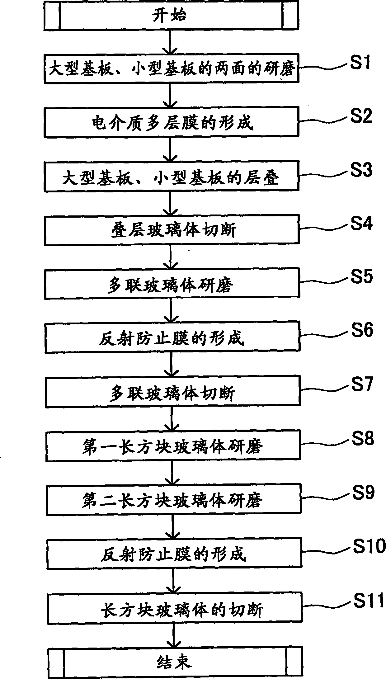
Figure 1 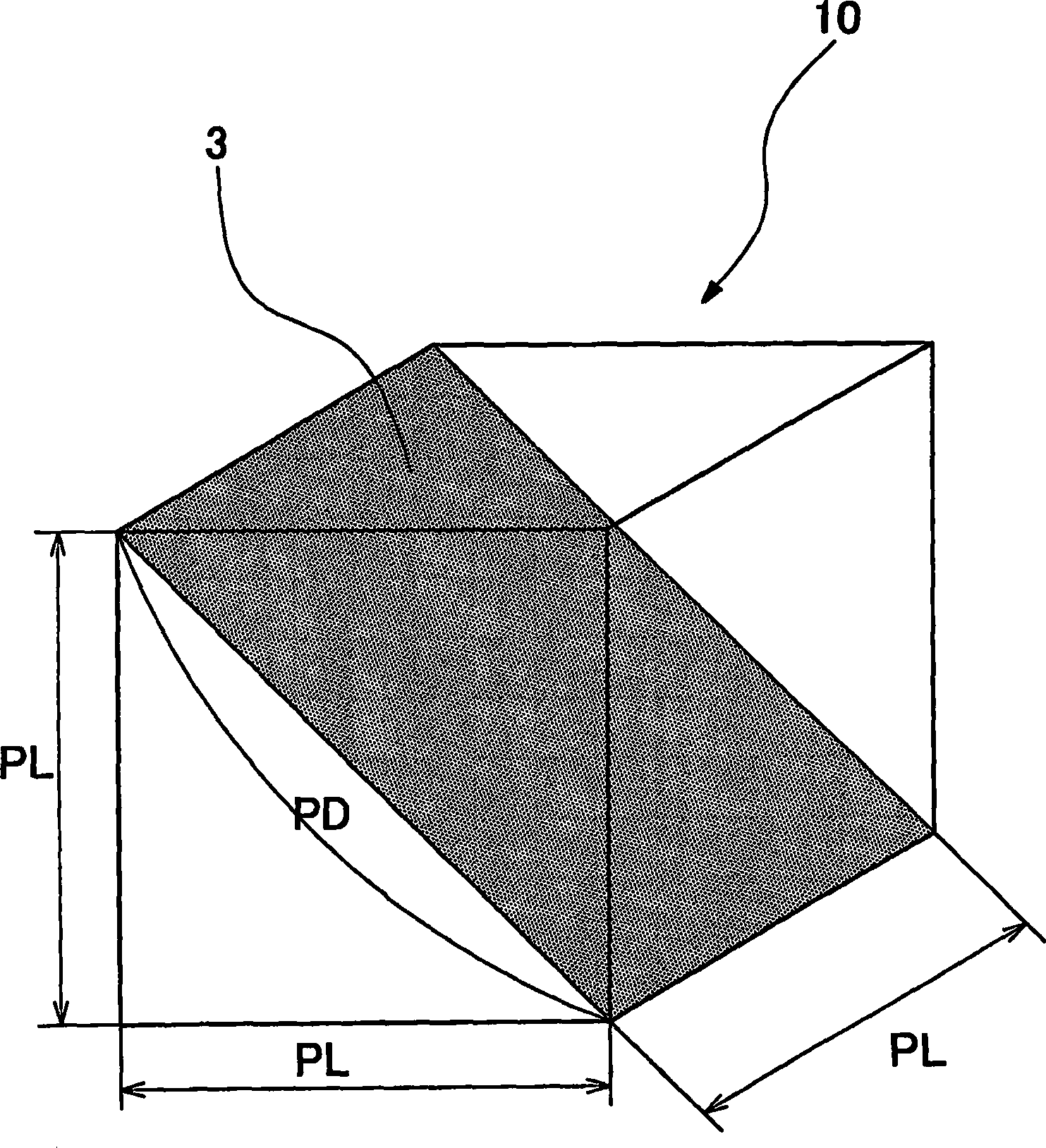
Figure 2 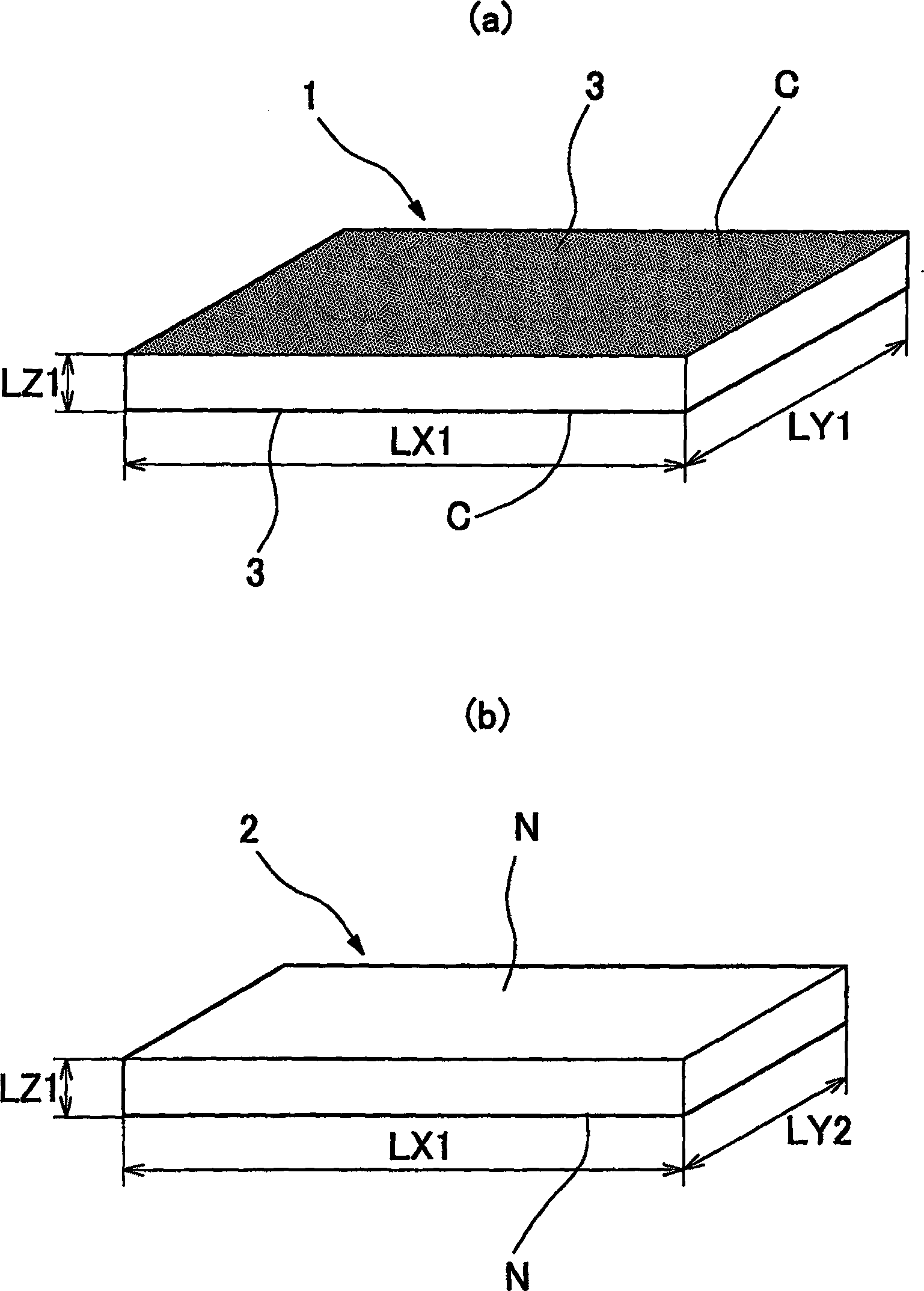
Figure 3
Abstract
Description
technical field
[0001] The invention relates to a method for manufacturing a prism. Background technique
[0002] A component of an optical system typified by an optical pickup device includes, for example, a polarizing beam splitter. The polarizing beam splitter is an optical element that separates the laser light emitted from the light source into reflected light and transmitted light. Either one of the reflected light and the transmitted light is directed to the optical disc, and the other is directed to the APC for detecting the intensity of the laser light. (Automatic power control) by light components. Since the reflected light reflected by the polarizing beam splitter is generally reflected at an angle of 90°, the polarized light separation film constituting the polarizing beam splitter is arranged at an angle of 45° to the optical axis. Therefore, a cube-shaped prism was used as the polarization beam splitter, and the polarization separation film was formed on the ...
Examples
Embodiment Construction
[0024] Below, according to figure 1 The flowchart of Figure 1 illustrates an embodiment of the invention. figure 2 It is the prism 10 finally manufactured. The prism 10 of this embodiment is a cubic optical element with one side PL long, and the dielectric multilayer film 3 is formed at an angle of 45° with respect to the optical axis. Here, in this embodiment, the diagonal length of each surface of the prism 10 (the long side of the surface on which the dielectric multilayer film 3 is formed) is defined as the diagonal length PD of the prism 10 (=PL×). In addition, an antireflection film having an antireflection function is formed on each surface of the prism 10 .
[0025] initially as image 3 As shown, a plurality of two types of flat substrates (substrates such as glass substrates) having different shapes are prepared. exist image 3 (a) shows a large substrate 1 having a long side (width) of LX1, a short side (depth) of LY1, and a thickness of LZ1. image 3 (b) sh...