
Memory unit, array and operation method thereof
Patent Information
- Authority / Receiving Office
- US · United States
- Patent Type
- Patents(United States)
- Current Assignee / Owner
- Publication Date
- 2022-11-08
Smart Images
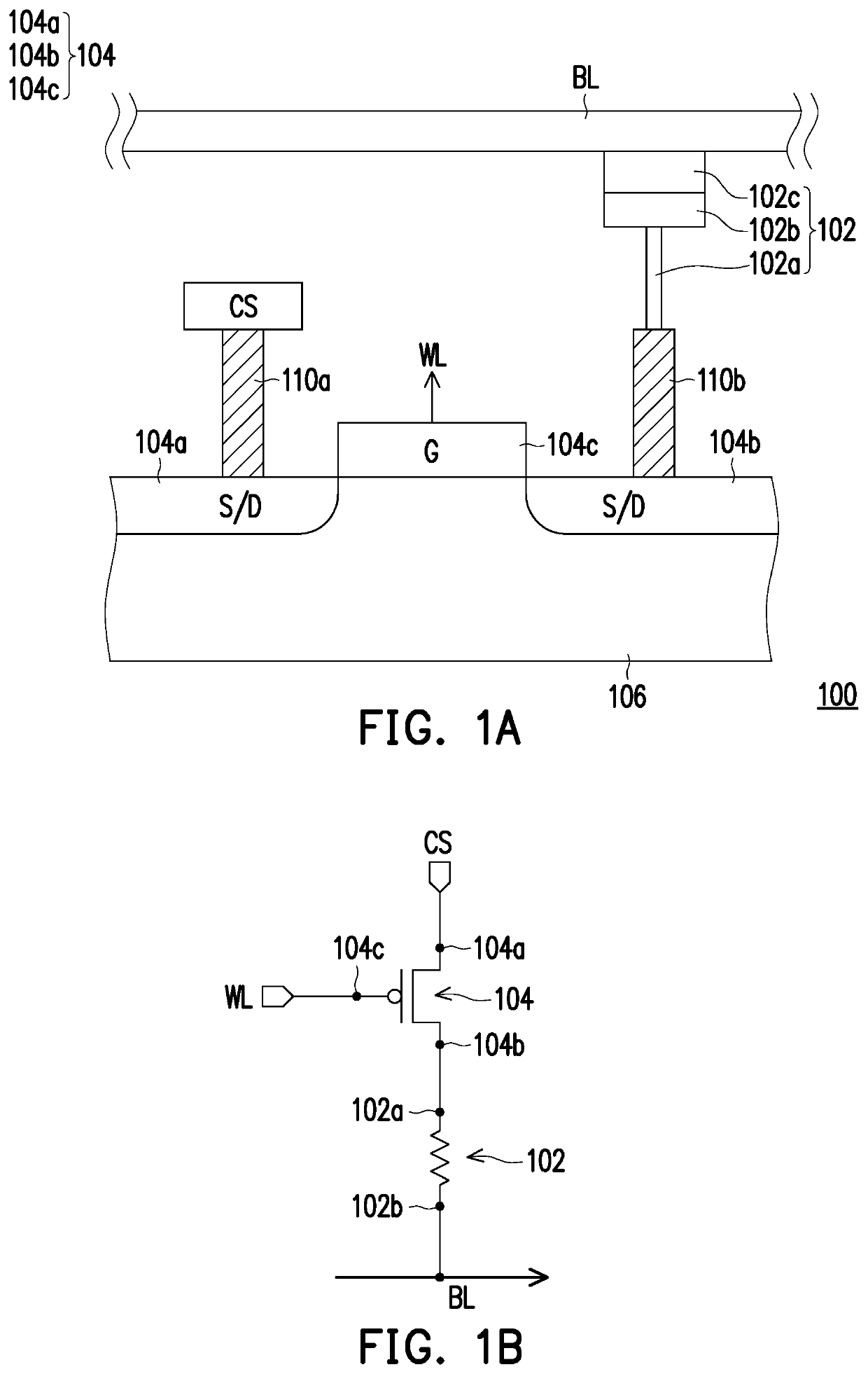
Figure 1 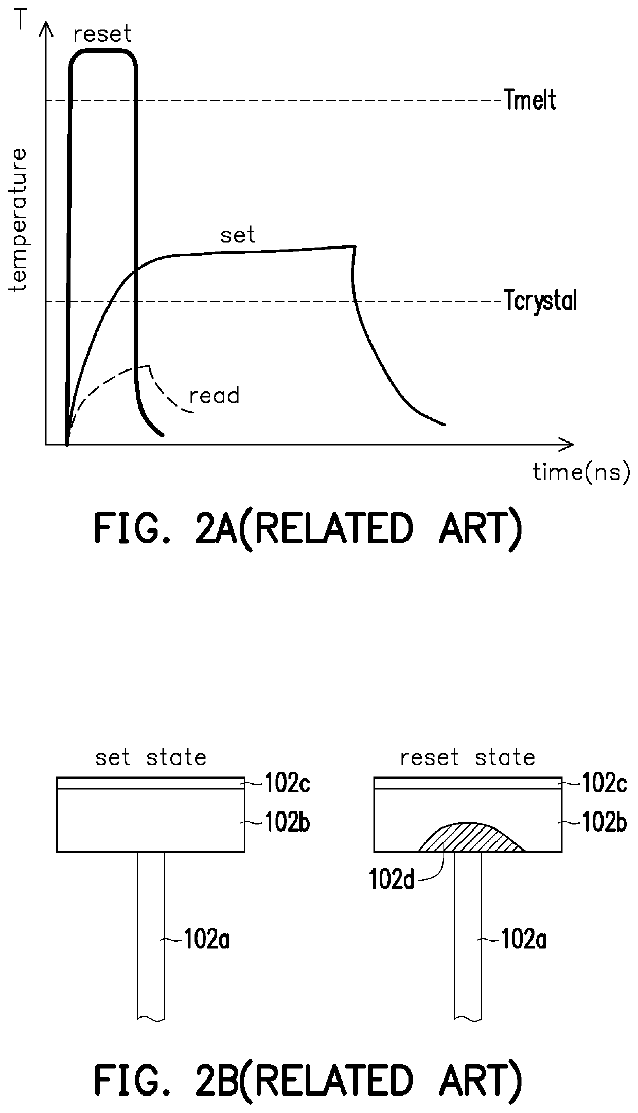
Figure 2 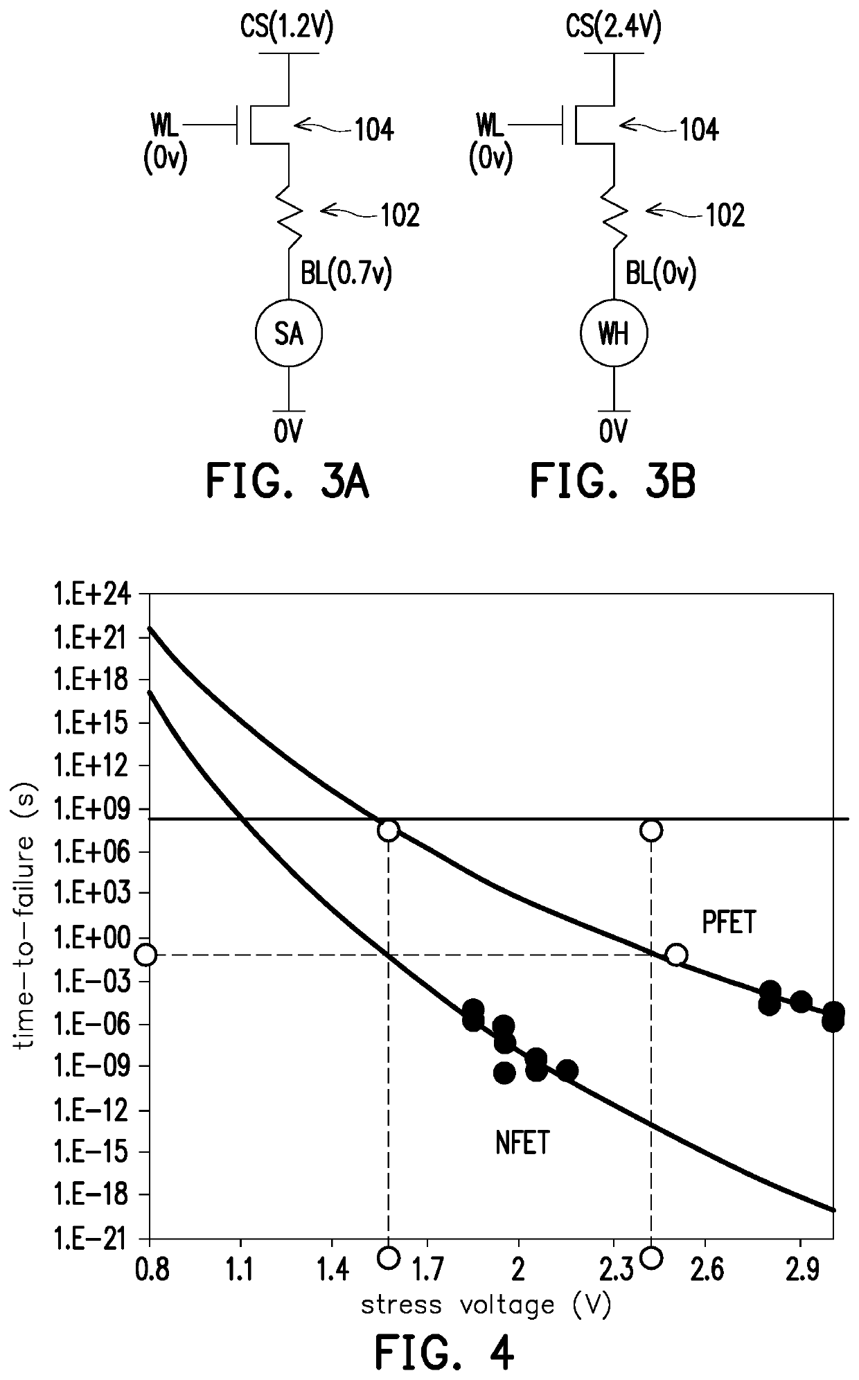
Figure 3
Abstract
Description
TECHNICAL FIELD
[0001] The present invention relates to a memory unit, an array, and an operation method thereof.DESCRIPTION OF RELATED ART
[0002] Phase change memory (PCM) uses changes in the phase of a material to achieve the characteristics of the memory. The phase change memory has the characteristics of small size and long storage time, and can also match the current semiconductor manufacturing technology.
[0003] In the current phase change memory structure, an NMOS transistor is usually used as the transistor of the driving element of each memory cell. However, when the process technology reaches the technical level of, for example, 14 nm, the gate electrode of the NMOS transistor is very thin and the breakdown voltage of the oxide layer is too low, making it difficult to be the driving element of the memory cell. Under the existing configuration, writing data to the memory cell requires applying a voltage of about 2.4V to the word line and about 2.5V to the bit line. However, due t...
Examples
Embodiment Construction
[0024]FIG. 1A shows a schematic diagram of a cross-sectional structure of a phase change memory unit according to one embodiment of the disclosure. As shown in FIG. 1A, the memory unit 100 comprises a memory cell (such as a variable resistor element) 102 and a driving element 104. In this embodiment, the memory cell 102 is made of phase change material but not limited thereto, and the driving element 104 may be a switching element, such as bipolar junction transistor (BJT), metal oxide semiconductor (MOS) transistor, field effect transistor (FET), diode, etc. In the embodiment, the driving element 104 is a P-type driving element, and a PMOS transistor is used as an example in the following description.
[0025]As shown in the cross-sectional view of FIG. 1, the memory unit 100 includes a PMOS transistor 104 with source-drains 104a, 104b and a gate 104c formed on a semiconductor substrate 106. In a memory array, a row of memory units 100 are connected by a word line WL, and the word lin...