
Optical semiconductor device and method of fabricating the same
a technology of optical semiconductor and semiconductor, applied in the direction of semiconductor laser structure details, semiconductor lasers, lasers, etc., can solve the problems of many electrons and holes, catastrophic optical damage of powerful laser diodes, and heat generated by laser diodes to damage the end surface of laser diodes, so as to achieve the effect of preventing components and improving cod
Patent Information
- Authority / Receiving Office
- US · United States
- Patent Type
- Applications(United States)
- Current Assignee / Owner
- Publication Date
- 2005-02-24
- Estimated Expiration
- Not applicable · inactive patent
Smart Images
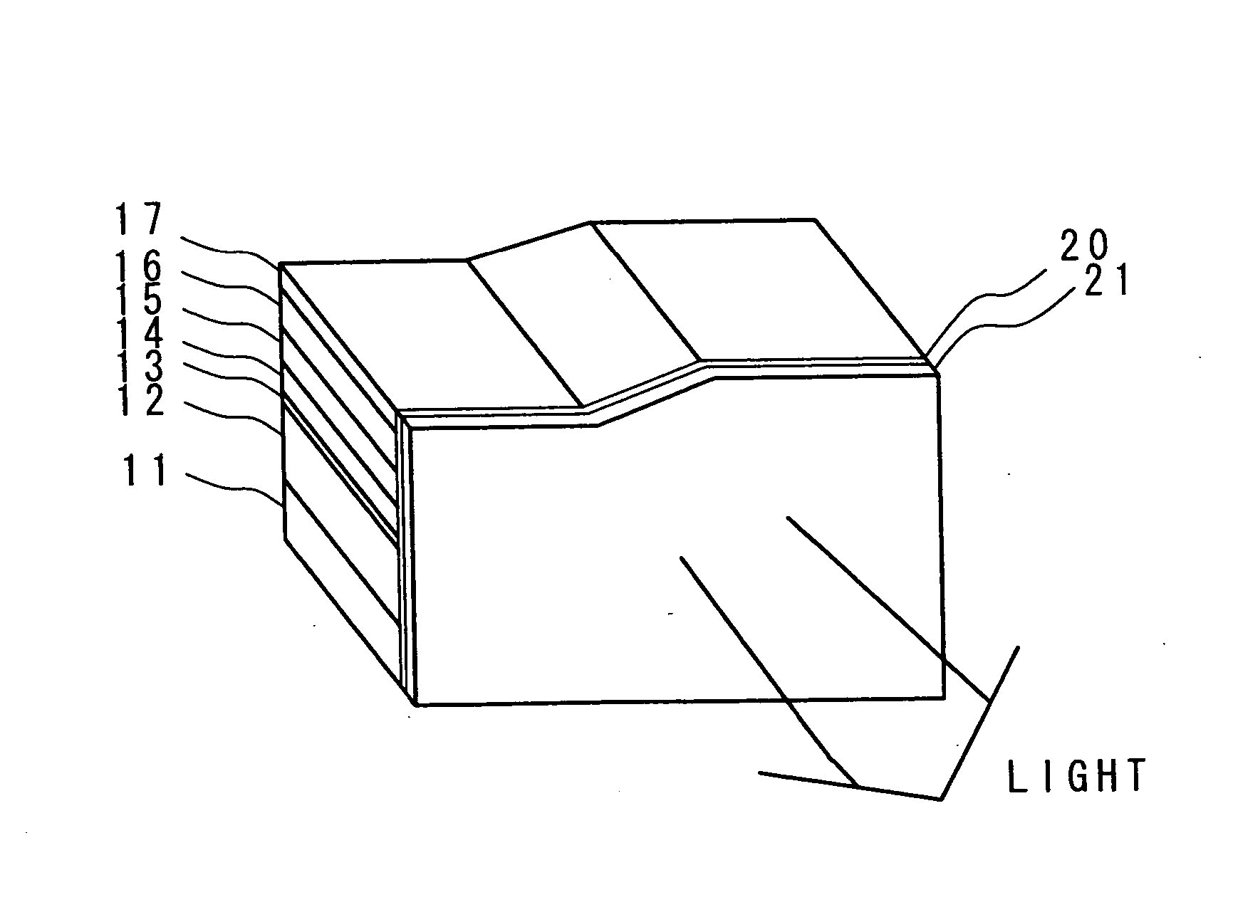
Figure 1 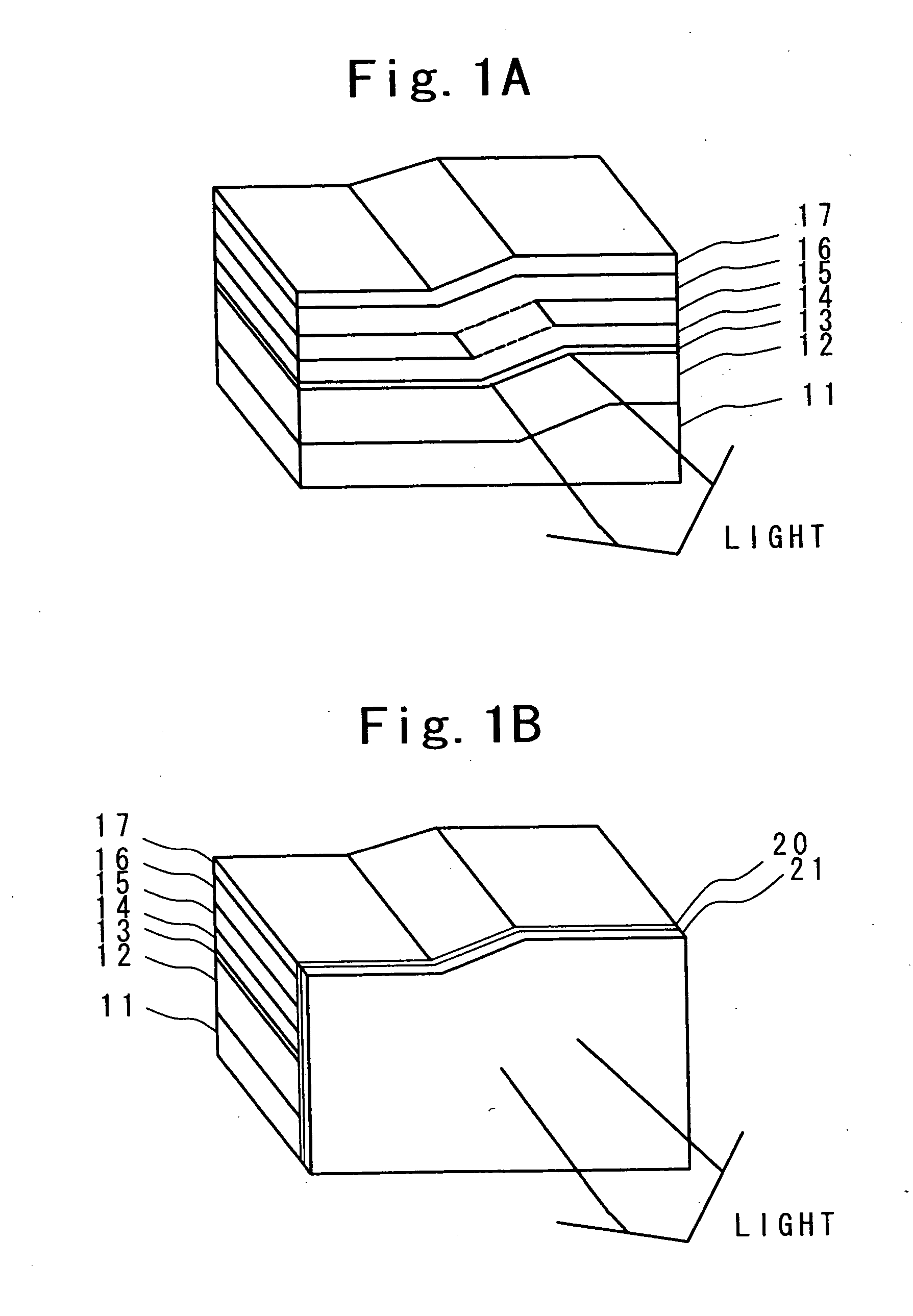
Figure 2 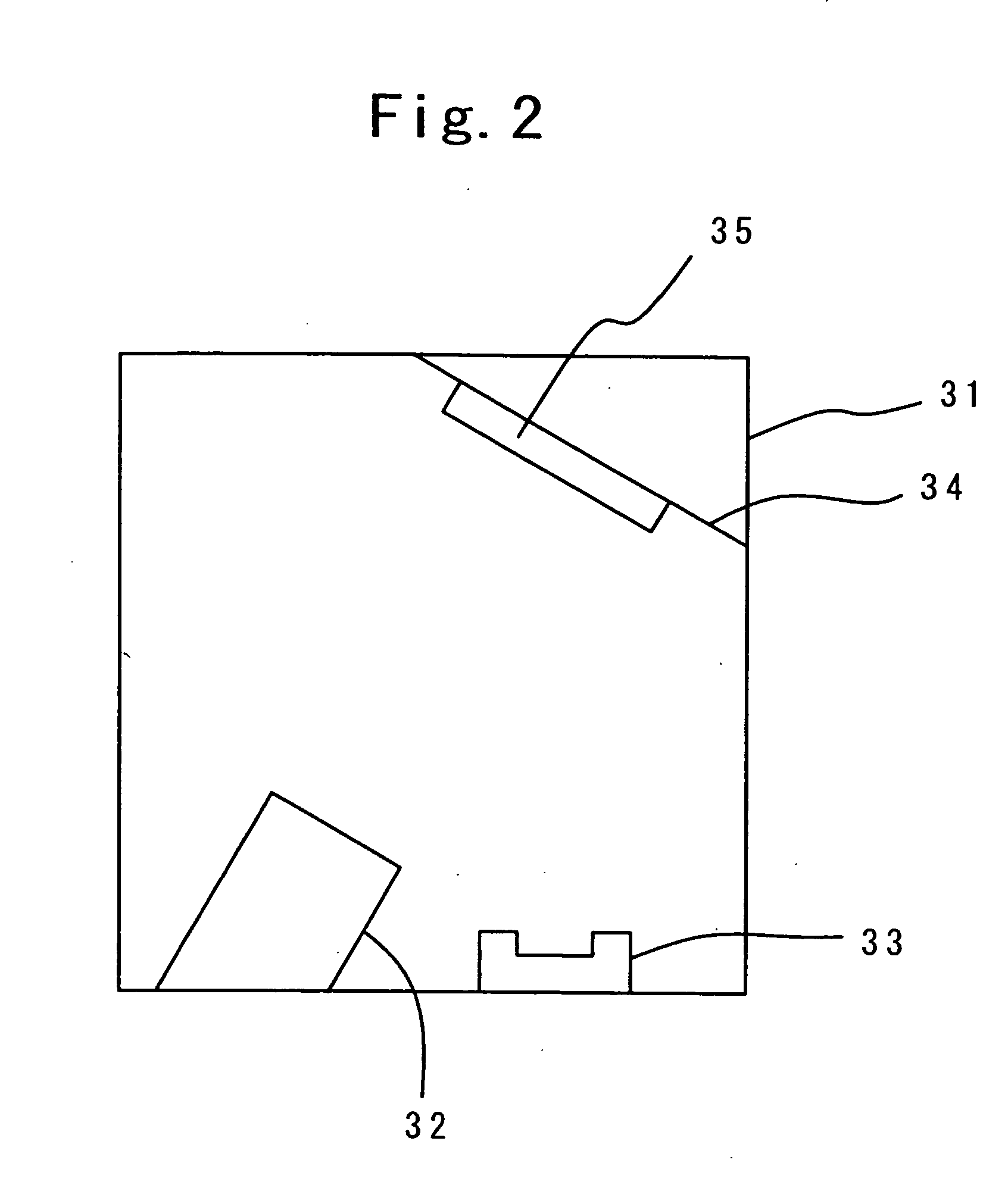
Figure 3
Abstract
Description
[0001] This application is a divisional of prior application Ser. No. 10 / 396,404 filed Mar. 26, 2003.BACKGROUND OF THE INVENTION
[0002] 1. Field of the Invention
[0003] The present invention generally relates to an optical semiconductor device and a method of fabricating the same, and more particularly, to the technique of forming a passivation film on an end surface of a semiconductor laser diode.
[0004] 2. Description of the Related Art
[0005] Recently, many types of high-power semiconductor laser diodes have been proposed. Powerful laser diodes have the problem of catastrophic optical damage (hereinafter simply referred to COD). Power up of the semiconductor laser diodes will not be realized unless a high COD level can be achieved. COD relates to the state of the end surface (facet) of the laser diode. If there is an impurity (for example, natural oxide film) or lattice defect exists on the end surface, light will be absorbed at such defective portions, this absorption resulting ...
Examples
Embodiment Construction
[0020] A description will now be given of an embodiment of the present invention with reference to the accompanying drawings.
[0021]FIG. 1A is a perspective view of a semiconductor laser diode, and FIG. 1B is a perspective view of a semiconductor laser diode provided by applying a passivation film of the present invention to the laser diode shown in FIG. 1A. The laser diode shown in FIG. 1A has a laminated layer structure, which includes a GaAs substrate 11, an n-type AlGaInP clad layer 12, an MQW (Multi Quantum Well) active layer 13, a first p-type AlGaInP clad layer 14, an AlGaInP current confinement layer 15, a second p-type AlGaInP clad layer 16, and a p-type GaAs contact layer 17. The AlGaInP current confinement layer 15 contains both p-type and n-type impurities. The current confinement layer 15 has a flat portion and a slope portion. The flat and slope portions have different incorporation rates of the impurities, so that the flat portion is of n type and the slope portion is...