
Method for fabricating a semiconductor device by transferring a layer to a support with curvature
Patent Information
- Authority / Receiving Office
- US · United States
- Current Assignee / Owner
- Publication Date
- 2005-07-28
- Estimated Expiration
- Not applicable · inactive patent
Smart Images
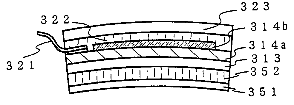
Figure 1 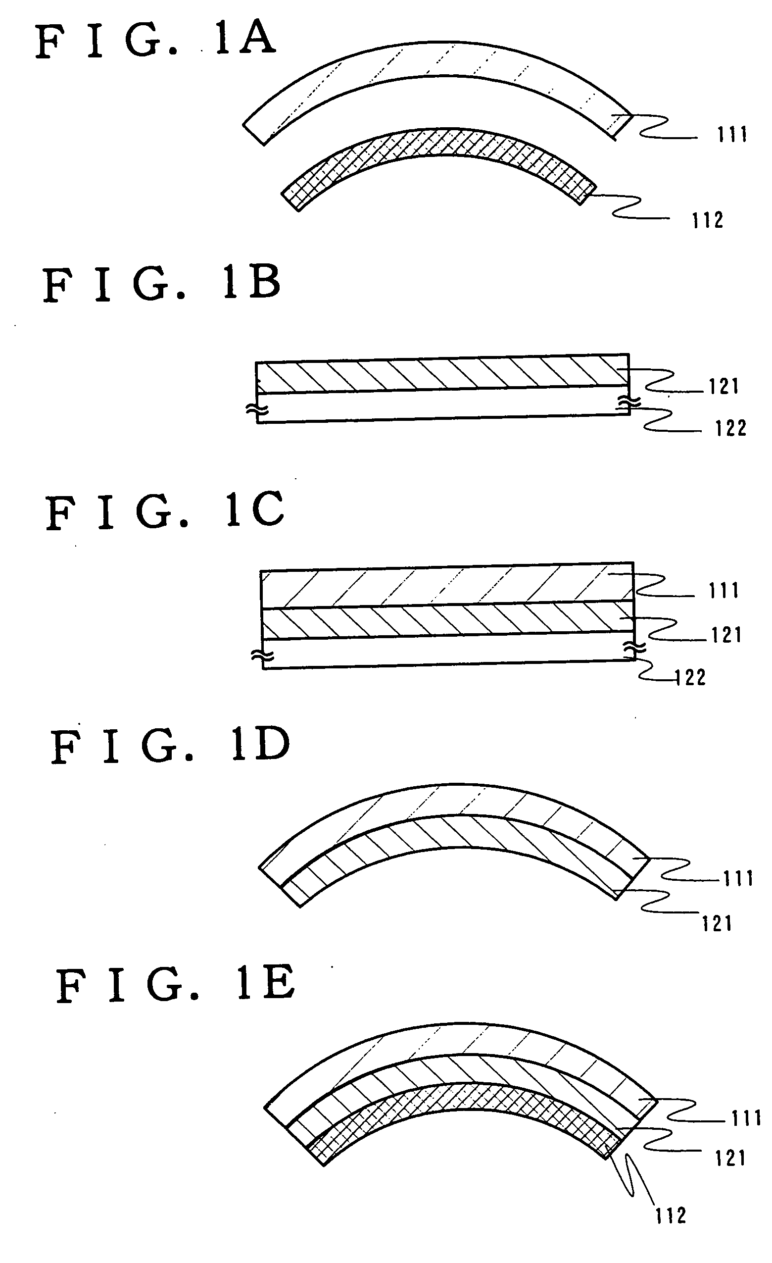
Figure 2 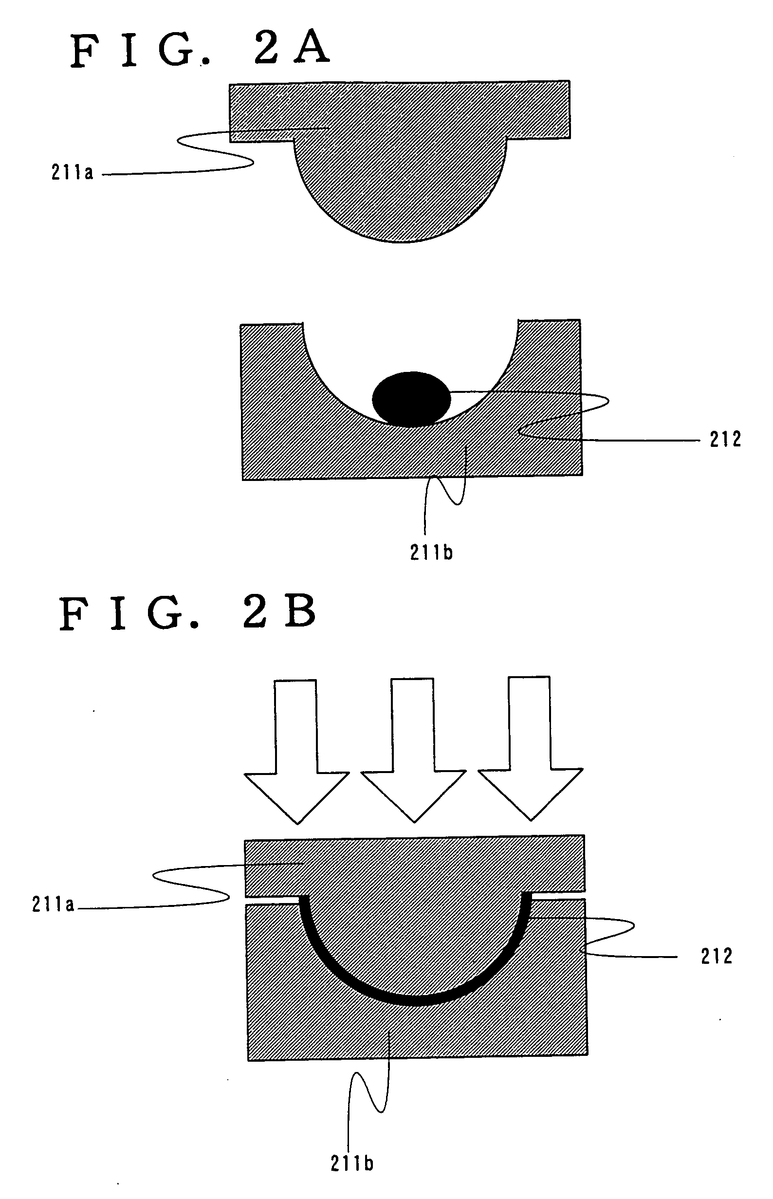
Figure 3
Abstract
Description
BACKGROUND OF THE INVENTION
[0001] The present invention relates to a method for fabricating a semiconductor device having a circuit configured of a thin film transistor (hereafter, it is called a TFT) in which a peeled layer that has been peeled is bonded and transferred to a base material, particularly to a method for transferring a circuit configured of a TFT to a support with curvature.
[0002] In recent years, a technique has been receiving attention in which a semiconductor thin film (a thickness of about a few to a few hundreds nanometers) formed over a substrate having an insulated surface is used to configure TFTs. The TFT is widely used for electronic devices such as ICs and electro-optic devices, which has been urged to develop as a switching device for image display devices.
[0003] In addition, an attempt has been made to install various display devices on vehicles such as automobiles and aircrafts, including display devices for navigation systems, operation screen displa...
Examples
embodiment
[Embodiment 1]
[0052] In the embodiment, the procedures to fabricate a light emitting device having an organic light emitting diode (OLED) are shown in FIGS. 3A to 3E.
[0053] As shown in FIG. 3A, a first material layer 312 is formed over a substrate 311. As the first material layer 312, it may have compressive stress or may have tensile stress immediately after the deposition. It is important to use materials that do not generate abnormality in peeling due to annealing in forming the peeled layer and the irradiation of laser light and have tensile stress in the range of 1 to 1×10¹⁰ (Dyne / cm2) after the peeled layer is formed. Typically, nitrides or metals are preferable. A representative example is a single layer formed of an element selected from W, WN, TiN and TiW, an alloy material or compound material having a principal component of the elements, or a laminated layer of these. In addition, it is fine to use sputtering for the first material layer 312.
[0054] For the substrate 31...
embodiment 2
[Embodiment 2]
[0073] In the embodiment, the procedures to fabricate a liquid crystal display device are shown in FIGS. 4A to 4E.
[0074] As shown in FIG. 4A, a first material layer 412 is deposited over the substrate 411. As the first material layer 412, it may have the compressive stress or may have tensile stress immediately after film deposition. However, it is important to use materials that do not generate abnormality in peeling due to annealing in forming the peeled layer and the irradiation of laser light and have the tensile stress in the range of 1 to 1×10¹⁰ (Dyne / cm2) after the peeled layer is formed. Typically, nitrides or metals are preferable. A representative example is a single layer formed of an element elected from W. WN, TiN and TiW, an alloy material or a compound material having a principal component of these elements, or a laminated layer of these. In addition, it is fine to use sputtering for the first material layer 412.
[0075] As the substrate 411, glass, sili...
embodiment 3
[Embodiment 3]
[0091] In the embodiment, FIG. 5 shows an apparatus for fabricating a light emitting device having an organic light emitting diode. In addition, the apparatus shown in the embodiment allows fabricating the light emitting device shown in the embodiment 1.
[0092]FIG. 5 shows an apparatus for depositing a light emitting layer (EL layer) of the organic light emitting diode by the dry deposition method of low weight molecular organic compounds. The apparatus is mainly configured of transport chambers for transferring substrates, delivery chambers for delivery, deposition chambers for depositing various thin films, and an encapsulation chamber for encapsulation. Each chamber is equipped with an exhaust system for achieving necessary vacuum degrees or a system for generating a gas atmosphere such as N2. In addition, the separate chambers are connected by gate valves. The substrates are transferred by transfer robots.
[0093] First, a substrate 501c necessary to fabricate an or...