
Non-volatile memory and method of manufacturing the same
Patent Information
- Authority / Receiving Office
- US · United States
- Current Assignee / Owner
- Publication Date
- 2005-12-15
- Estimated Expiration
- Not applicable · inactive patent
Smart Images
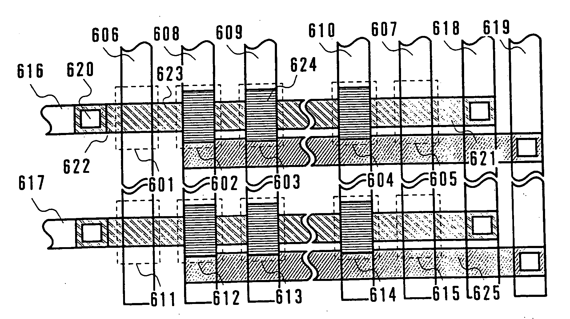
Figure 1 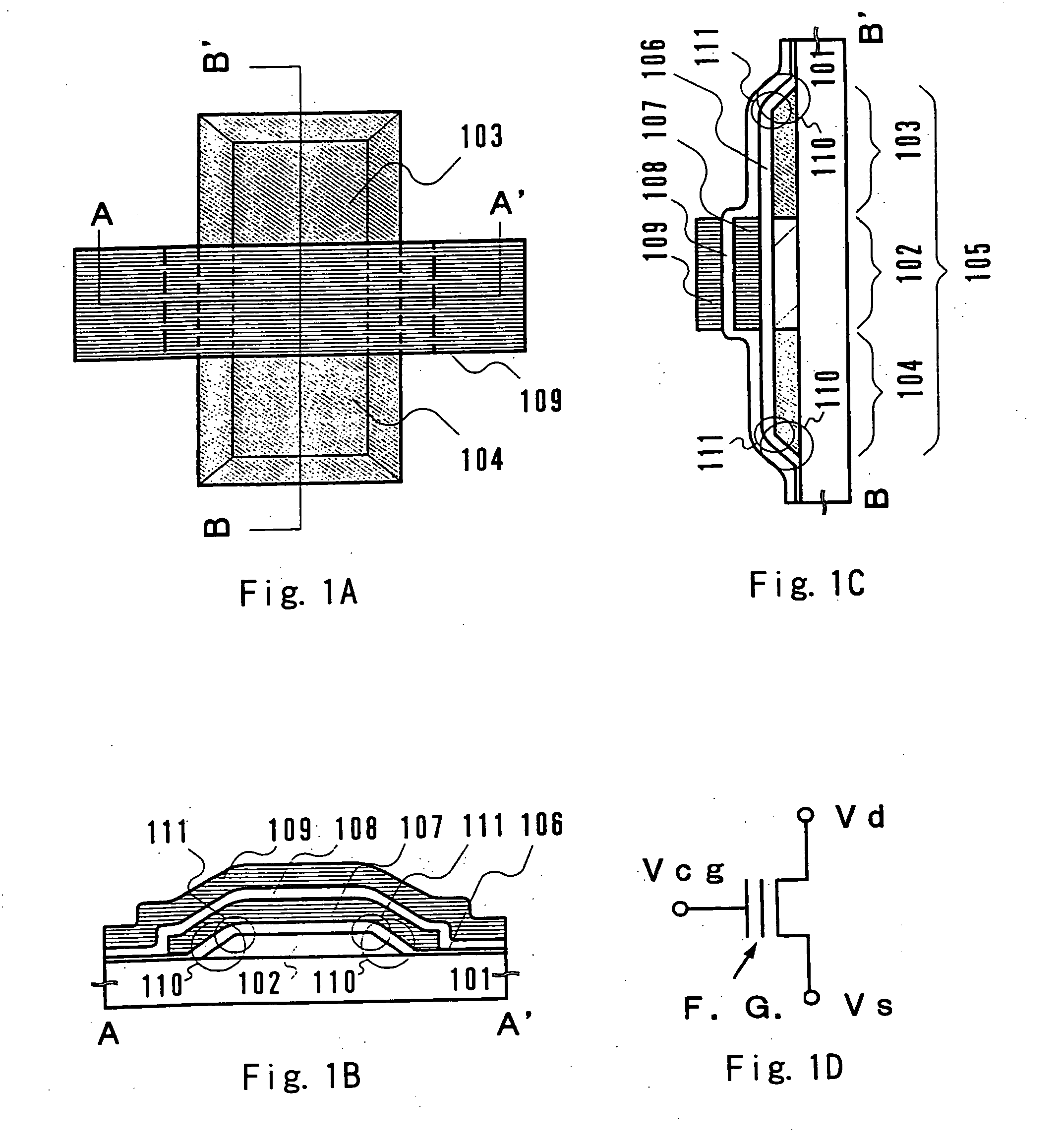
Figure 2 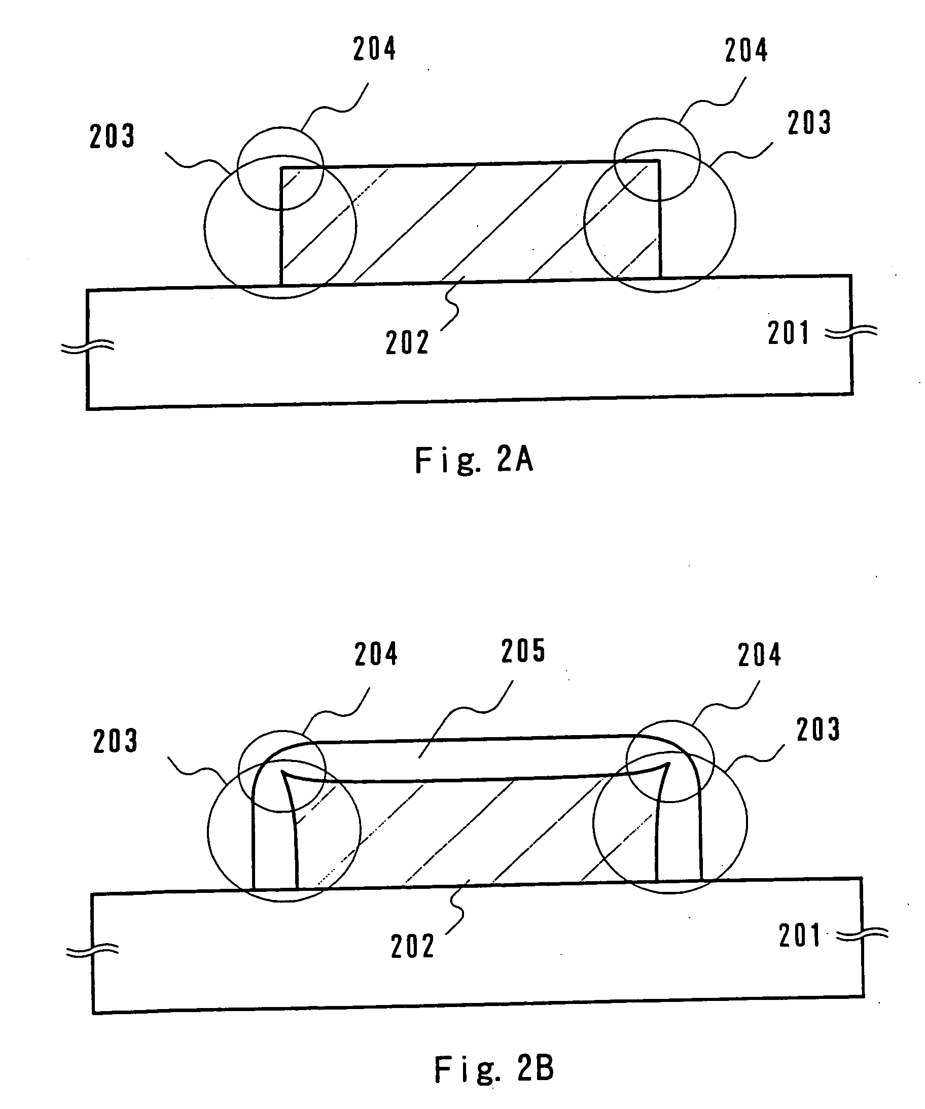
Figure 3
Abstract
Description
BACKGROUND OF THE INVENTION
[0001] 1. Field of the Invention
[0002] The present invention relates to a non-volatile memory using a thin film transistor (TFT) and to a method of manufacturing the non-volatile memory.
[0003] 2. Description of Related Art
[0004] The technique for forming a semiconductor thin film on an insulating substrate, especially the one for forming a silicon thin film on a glass substrate, is advancing at a remarkable pace in recent years. Conventionally, an insulated gate field effect transistor such as a MOS FET is formed on a single crystal semiconductor substrate. A TFT that has as its active layer a semiconductor thin film formed on an insulating substrate is expected to have low parasitic capacitance, high operation-speed, less power consumption, and a low manufacturing cost. Great hopes are laid on a system-on-glass in which those characteristics of TFT are utilized to integrate a system LSI on a glass substrate. To realize the system-on-glass, it is indis...
Examples
embodiment 1
[Embodiment 1]
[0056] This embodiment describes a method of manufacturing an n type memory TFT that has the structure shown in Embodiment Mode.
[0057]FIGS. 4A to 4E are sectional views each showing a major manufacturing step for manufacturing the n type memory TFT according to Embodiment Mode. These sectional views are taken along the line A-A′ in FIG. 1A.
[0058] First, a polycrystalline silicon thin film 402 with a thickness of 500 angstrom is formed on a substrate 401 having an insulating surface as shown in FIG. 4A. A quartz substrate, a silicon substrate with a thermal oxide film formed thereon, a ceramic substrate with a base film formed thereon, or the like can be used as the substrate 401 having an insulating surface. In this embodiment, a quartz substrate is employed.
[0059] The polycrystalline silicon thin film 402 may be formed directly by CVD apparatus or may be obtained by crystallizing an amorphous silicon thin film. When crystallizing amorphous silicon, any of furnace a...
embodiment 2
[Embodiment 2]
[0078] This embodiment describes a method of manufacturing a non-volatile memory in which active layer side ends are tapered and tiered to have two or more tiers.
[0079] The manufacturing steps of Embodiment 1 are employed here for steps from formation of a semiconductor thin film on a substrate having an insulating surface through formation of a photo resist having an active layer pattern. In the subsequent step of etching the semiconductor thin film, active layer side ends are tapered to have two tiers. The taper angle of the active layer side ends is set such that the upper tier has a smaller taper angle (preferably 20 to 50°) and the lower tier has a larger taper angle (preferably 40 to 70°). This prevents the active layer side ends from being pointed at the interface between the substrate having an insulating surface and the active layer.
[0080] The active layer side ends can be tapered to have two tiers by changing the selective ratio of the semiconductor thin fi...
embodiment 3
[Embodiment 3]
[0087] A memory TFT of the present invention can be applied to any known circuit structure that uses a non-volatile memory element. This embodiment describes a case of applying the present invention to a NOR flash memory.
[0088]FIG. 5A is a circuit diagram of a NOR flash memory circuit in which memory TFTs are arranged so as to form a matrix having m rows and n columns (m and n are integers each equal to or larger than 1). The conductivity type of the memory TFTs is either n type or p type.
[0089] In FIG. 5A, m memory TFTs 502 to 504 in the first column are connected to a bit line 501 indicated by B1. The m memory TFTs 502 to 504 respectively use as control gates m word lines 505 to 507 indicated by W1 to Wm. Similarly, m memory TFTs 509 to 511 in the n-th column are connected to a bit line 508 indicated by Bn. The m memory TFTs 509 to 511 respectively use as control gates the m word lines 506 to 507. In the memory TFTs 502 to 504 and 509 to 511, the terminals that are...