
Method for chemical vapor deposition in high aspect ratio spaces
Patent Information
- Authority / Receiving Office
- US · United States
- Current Assignee / Owner
- Publication Date
- 2006-12-28
Smart Images
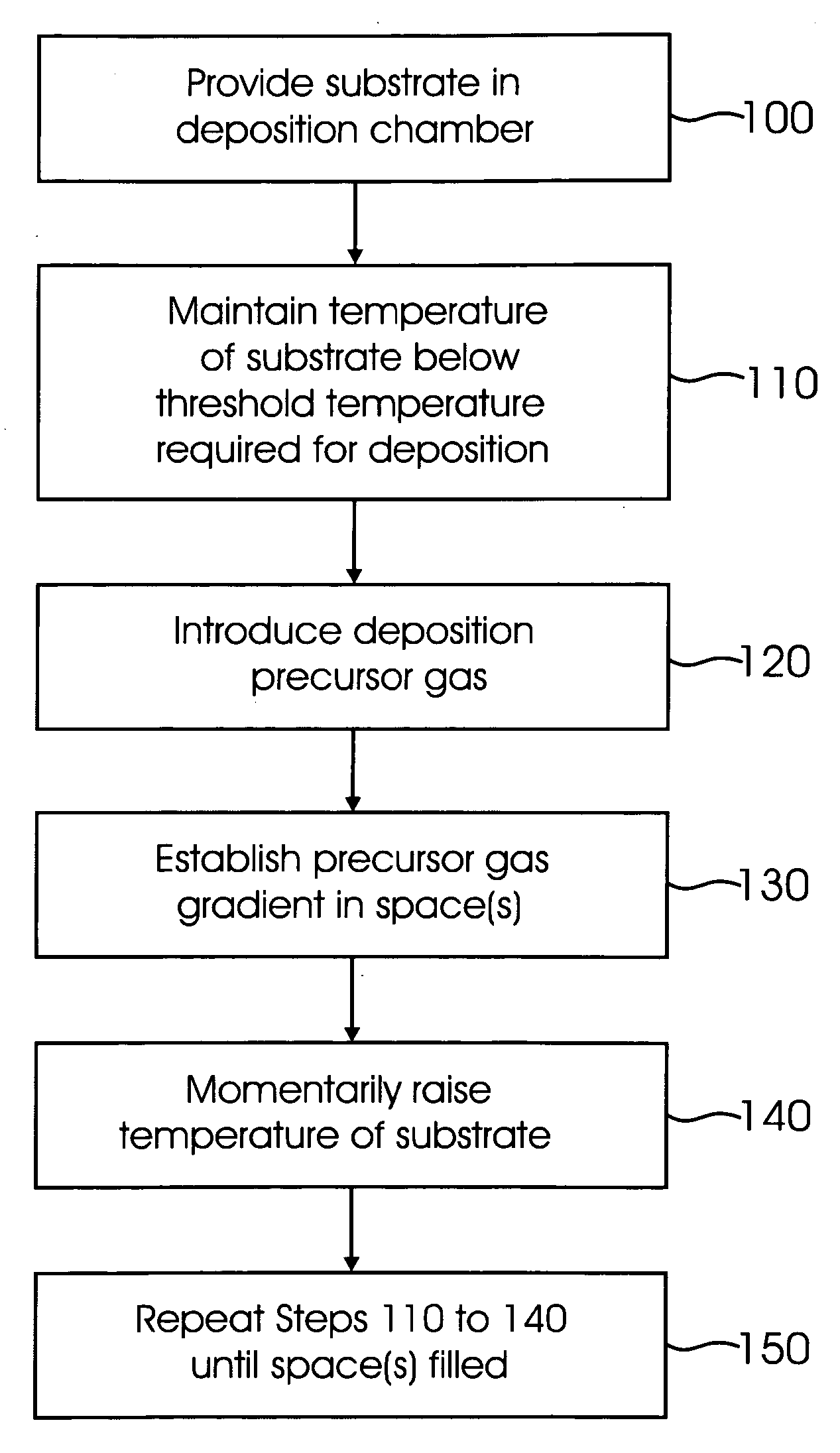
Figure 1 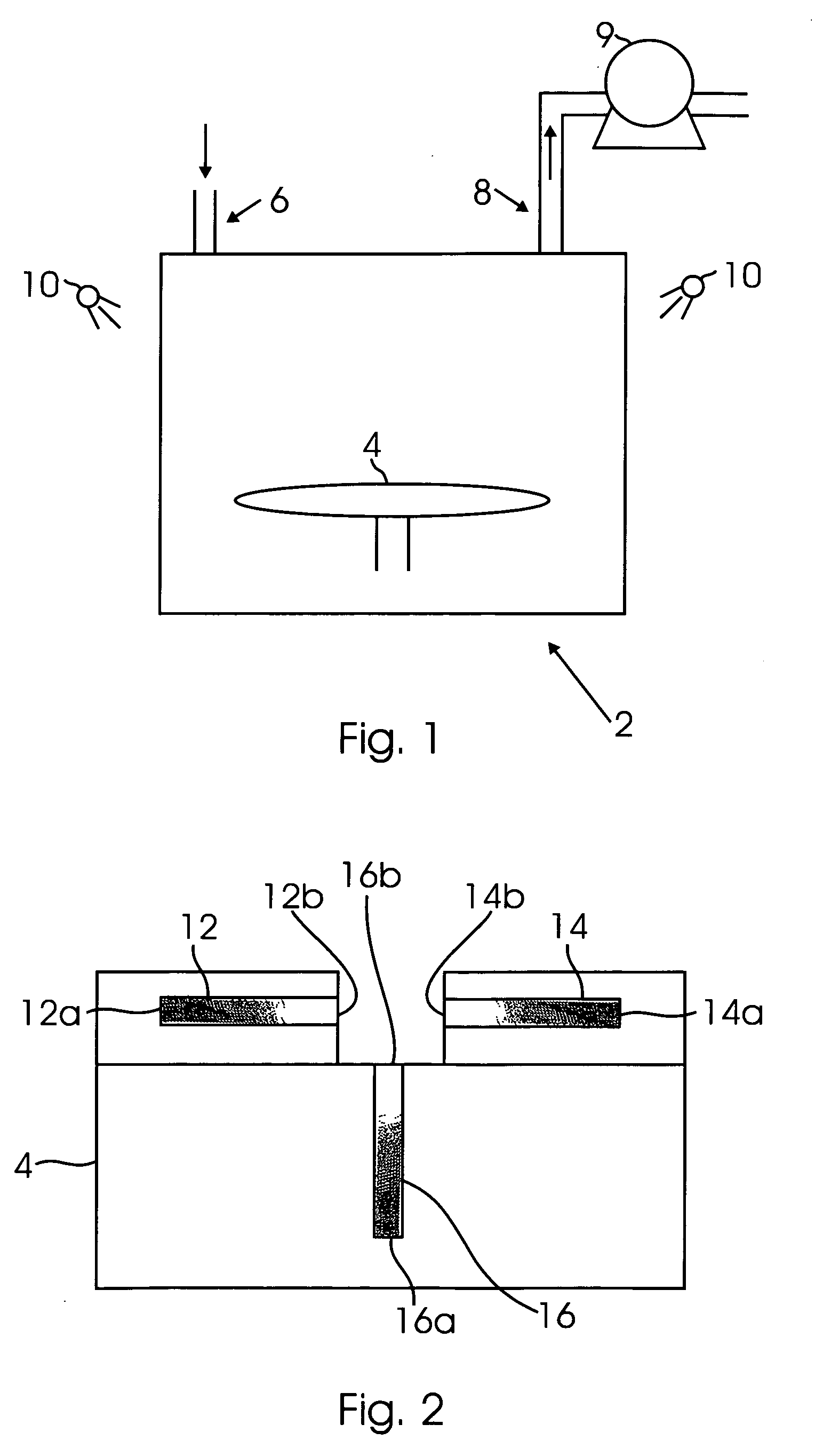
Figure 2 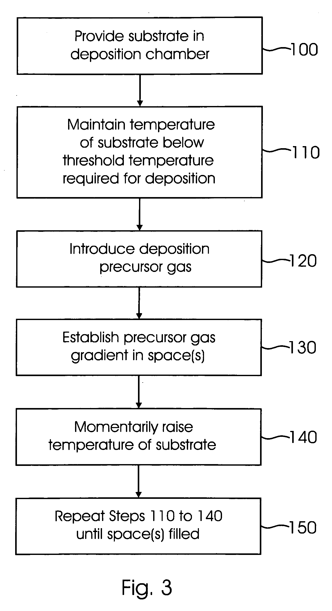
Figure 3
Abstract
Description
FIELD OF THE INVENTION
[0001] The field of the invention generally relates to methods of depositing conformal films on substrates. In particular, the field of the invention relates to methods of depositing conformal films on or into high aspect ratio spaces such as, for example, gaps, vias and trenches. BACKGROUND OF THE INVENTION
[0002] The semiconductor industry is increasingly being driven to decrease the size of semiconductor devices located on integrated circuits. For example, miniaturization is needed to accommodate the increasing density of circuits necessary for today's semiconductor products. The rapid advancement of silicon-based integrated circuit technology brings along the increasingly stringent requirement on the ability of depositing film into spaces having high aspect ratios, e.g. spaces where the ratio of the longest dimension to the shortest dimension is greater than 10. Many semiconductor devices include, for example, vias, gaps, trenches or other structures that ...
Examples
Embodiment Construction
[0020]FIG. 1 illustrates a deposition chamber 2 used for chemical vapor deposition of conformal films. The deposition chamber 2 may be a chamber used, for example, in low pressure chemical vapor deposition (LPCVD) and / or rapid temperature chemical vapor deposition (RTCVD). The deposition chamber 2 is preferably able to rapidly change pressure in response to a user input or control algorithm. The deposition chamber 2 illustrated in FIG. 1 includes a substrate 4 therein. Of course, multiple substrates 4 may be located inside the deposition chamber 2. The substrate 4 may comprise substrate material commonly used in integrated circuit technology and / or MEMS devices. The substrate 4 may comprise silicon or other semiconductor material. The substrate 4 may include active regions that need to be separated or otherwise isolated from one another, e.g., transistors separated by trenches or other isolation structures.
[0021] The deposition chamber 2 preferably includes one or more inlets 6 and...