
Low Noise Amplifier
Patent Information
- Authority / Receiving Office
- US · United States
- Patent Type
- Applications(United States)
- Current Assignee / Owner
- Publication Date
- 2009-07-02
Smart Images
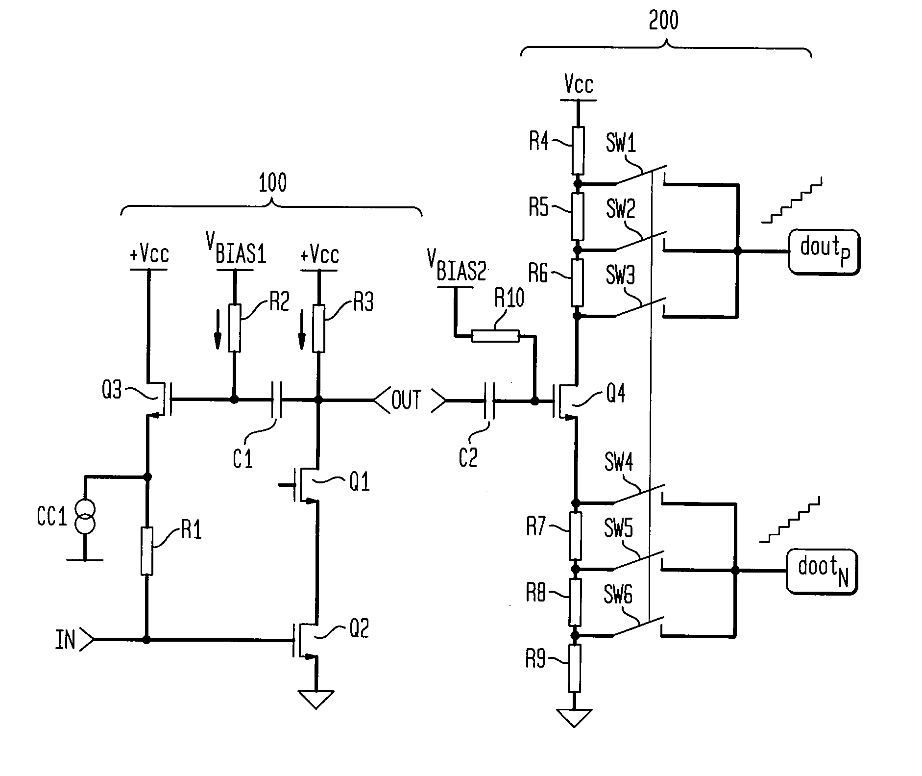
Figure 1 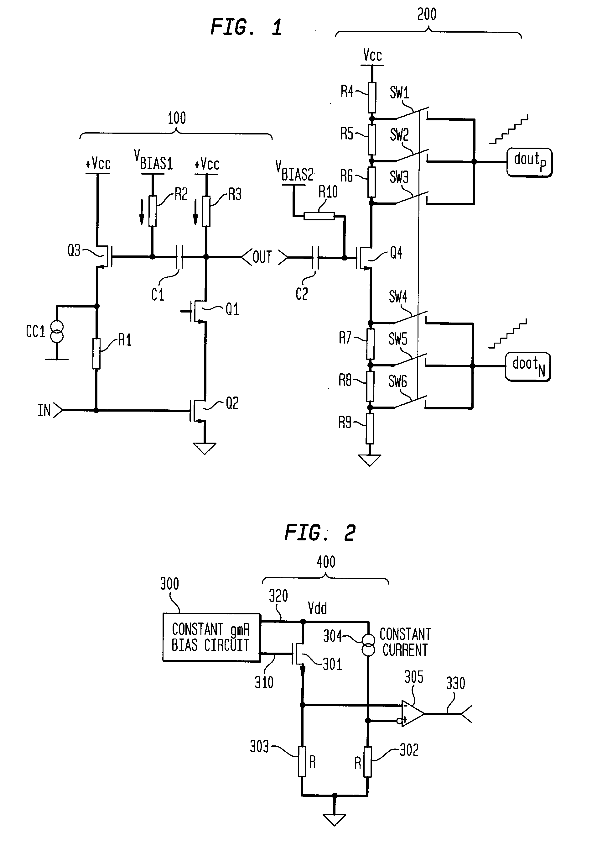
Figure 2
Abstract
Description
TECHNICAL FIELD OF THE INVENTION
[0001] The invention relates to an amplifier (LNA) such as a low noise amplifier.BACKGROUND OF THE INVENTION
[0002] A low noise amplifier (LNA) is a type of electronic amplifier used in communication systems to amplify very weak signals captured by an antenna.
[0003] One of the known issues with the prior art low noise amplifiers is to ensure that the low noise amplifiers have sufficient headroom at the output to ensure that an amplified input signal is not saturated at the output. In the prior art this can be achieved by providing a bank of selectable resistors between an output node and a voltage supply. One or more resistors can be selected in order to ensure that an output signal at the output node is not saturated.SUMMARY OF THE INVENTION
[0004] The invention discloses an amplifier with an input coupled to the gate of a second transistor and an output coupled to an output node between a third resistor and the drain of the second transistor. A third t...
Examples
Embodiment Construction
[0011]FIG. 1 illustrates an example of a low noise amplifier 100 and a conversion stage 200 according to an aspect of the invention. The low noise amplifier 100 of FIG. 1 is an example of a common-source amplifier in which the input signal IN is applied to the gate of a second transistor Q2 to control the signal-drain current. The output signal OUT is sensed across a third resistor R3 which is connected between a supply voltage Vcc and the drain of the transistor Q2. The third resistor R3 can be replaced by a bank of resistors which can be selected and act as a coarse gain for the low noise amplifier 10. Typically the selection of the resistors allows the course gain to be selected in steps of 6 dB, but this is not limiting of the invention. A first transistor Q1 is placed between the third resistor R3 and the drain of the second transistor Q2. The first transistor Q1 is a cascade transistor as known in the art and is used to isolate parasitic capacitance associated with the second ...