
Semiconductor device
Patent Information
- Authority / Receiving Office
- US · United States
- Current Assignee / Owner
- Publication Date
- 2010-09-02
- Estimated Expiration
- Not applicable · inactive patent
Smart Images
Figure 1 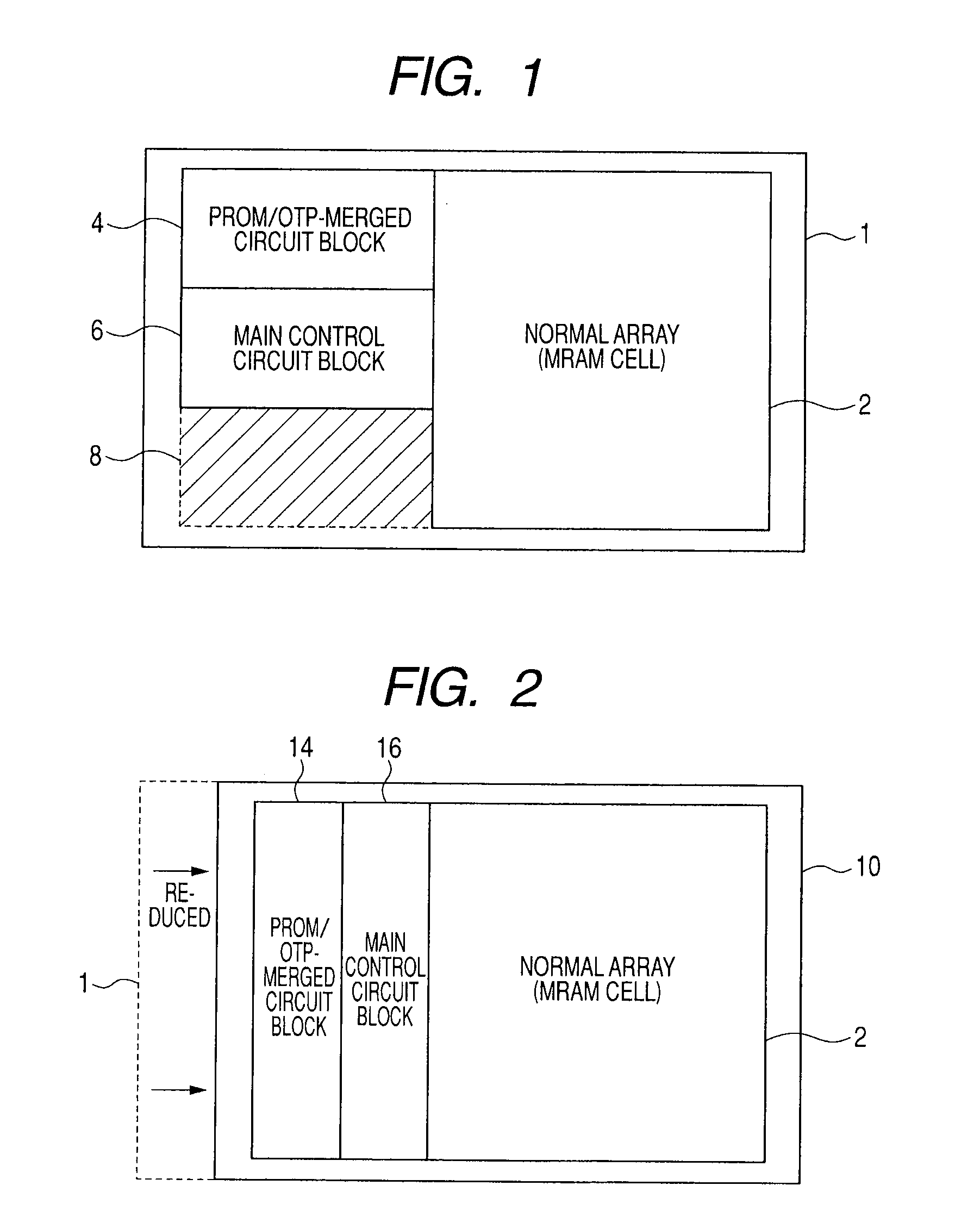
Figure 2 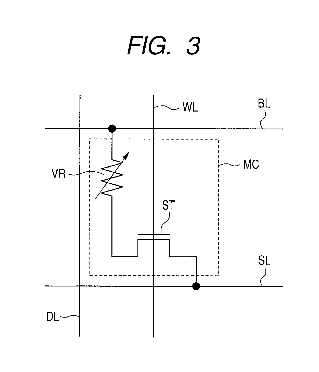
Figure 3
Abstract
Description
CROSS REFERENCES TO RELATED APPLICATIONS
[0001] The disclosure of Japanese Patent Application No. 2009-45815 filed on Feb. 27, 2009 and Japanese Patent Application No. 2009-208331 filed on Sep. 9, 2009 each including the specification, drawings and abstract are incorporated herein by reference in its entirety.BACKGROUND OF THE INVENTION
[0002] The present invention relates to a semiconductor device, in particular, to configuration of a storage unit which stores internal operation environment setup data, such as trimming data and repair data, in a nonvolatile manner. More specifically, the present invention relates to a magnetic semiconductor memory unit in the semiconductor device which utilizes a variable magnetoresistive element as a data storage element.
[0003] One of the nonvolatile semiconductor memories which store data in a nonvolatile manner includes a magnetic semiconductor memory (MRAM). The MRAM utilizes a variable magnetoresistive element, such as an MTJ element (magnetic tunn...
Examples
embodiment 1
[0083]FIG. 1 illustrates roughly a chip layout of a nonvolatile memory unit of a semiconductor device according to the present invention. In FIG. 1, the nonvolatile memory unit of the semiconductor device is an MRAM including an MRAM cell which utilizes a variable magnetoresistive element as a data storage element.
[0084]In FIG. 1, a normal array 2 is arranged over a semiconductor chip region 1 in the shape of a rectangle. In the normal array 2, MRAM cells are arranged in a matrix and hold data which is accessible from the exterior. The present semiconductor chip region 1 may be a chip as a single body, or may be a macro area which is a part of area over a semiconductor chip and forms a part of a system LSI.
[0085]Adjoining to the normal array 2, a PROM / OTP-merged circuit block 4 and a main control circuit block 6 are arranged in a rectangle area, respectively. The PROM / OTP-merged circuit block 4 includes a common MRAM cell array and operates as either PROM or OTPROM (hereafter simply...
embodiment 2
[0273]FIG. 30 is a drawing illustrating configuration of the principal part of a PROM / OTP-merged circuit according to Embodiment 2 of the present invention with cell structure of a normal array. In FIG. 30, a memory cell MC comprises a series body of a variable magnetoresistive element VR and a select transistor ST in a PROM / OTP array 40. The gate insulating film of the select transistor ST has a film thickness of Tox1.
[0274]On the other hand, in a bit-line write drive circuit 70, an OTP write drive circuit which performs data writing in an OTP mode is illustrated. In the OTP write drive circuit, a CMOS transmission gate 170 and a write column selection gate 172 are coupled in series between a bit line BL and a node which supplies a high bit-line writing voltage VREFBL. The CMOS transmission gate 170 includes a parallel body of a P-channel MOS transistor PT and an N-channel MOS transistor NT1, and write control signals TGEN_CEL and ZTGEN_CEL are supplied to the respective gates.
[027...
embodiment 3
[0393]FIG. 58 is a flow chart illustrating operation of a semiconductor device according to Embodiment 3 of the present invention. Hereafter, with reference to FIG. 58, operation of the semiconductor device according to Embodiment 3 of the present invention is explained.
[0394]After completion of manufacturing process of a semiconductor integrated circuit device, a wafer-level test is conducted (Step SS1). In the wafer-level test, a pad over a chip is exposed, and various characteristic tests are conducted by contacting a test probe to the pad. Detection of a bad cell of a memory cell, etc. are also performed by applying test data. In the first test, a test is carried out according to a default value of operating environment setup data.
[0395]In the test, test result data about each test item is collected (Step SS2). After the completion of the wafer-level test, it is determined whether a semiconductor device under test is a nondefective article which satisfies specification values et...