
Flexible semiconductor device and method for manufacturing the same
a technology of flexible semiconductors and semiconductors, applied in the direction of semiconductor devices, electrical equipment, transistors, etc., can solve the problems of peeling step of the substrate, lack of flexibility and breakage, and high price of the display panel, and achieve good densification properties, good smoothness, and thin thickness
Patent Information
- Authority / Receiving Office
- US · United States
- Patent Type
- Applications(United States)
- Current Assignee / Owner
- Publication Date
- 2011-02-24
Smart Images
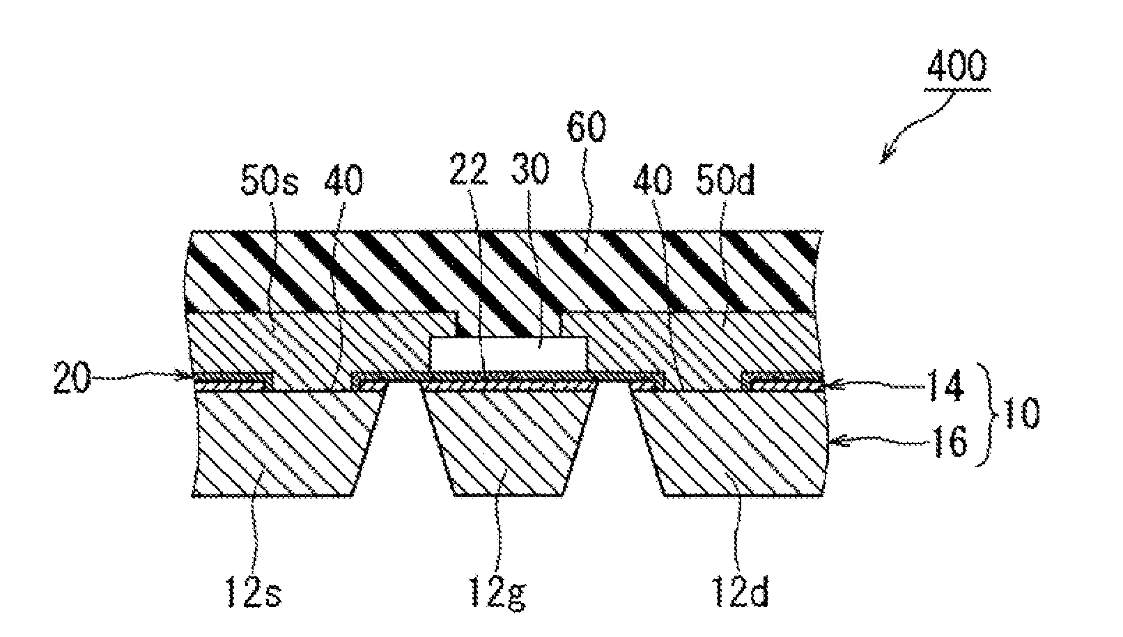
Figure 1 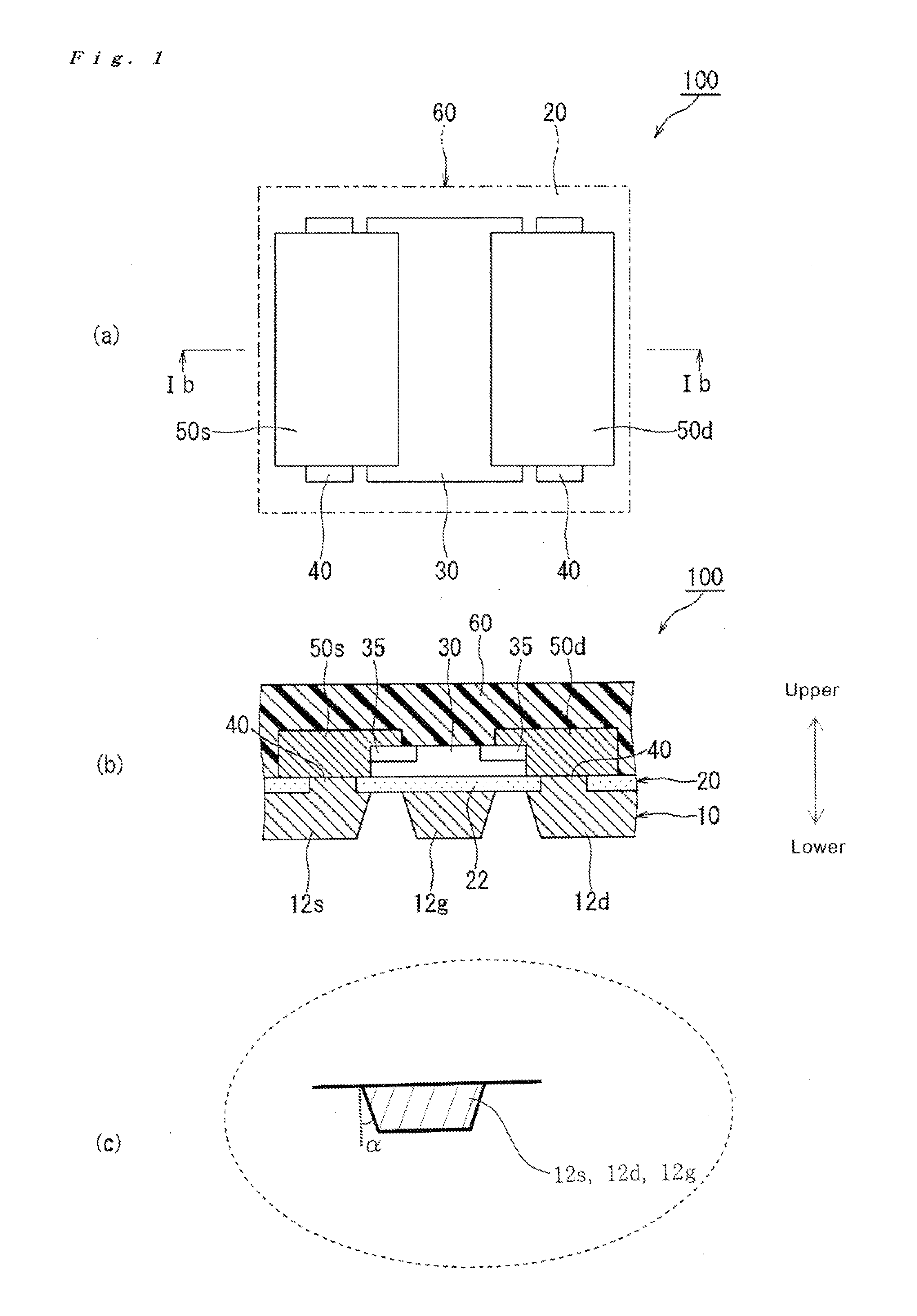
Figure 2 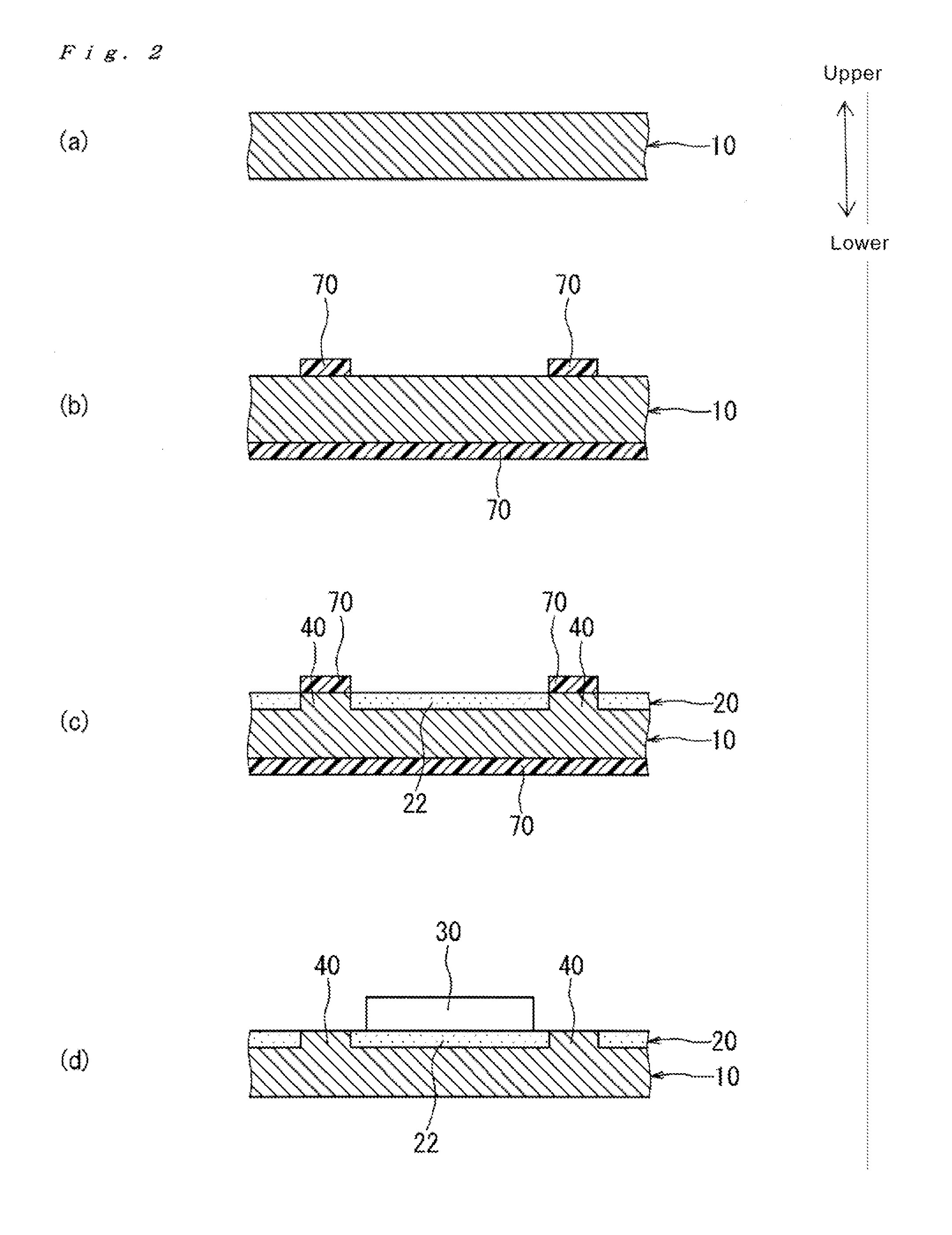
Figure 3
Abstract
Description
TECHNICAL FIELD
[0001] The present invention relates to a flexible semiconductor device with its flexibility, and also a method for manufacturing the same. In particular, the present invention relates to the flexible semiconductor device which can be used as a TFT, and also the method for manufacturing the same.BACKGROUND OF THE INVENTION
[0002] There is a growing need for a flat-panel display as an image display device with a wide spreading use of information terminals. With further advancement of informatization, there are also increasing opportunities in which information, which has been conventionally provided by paper medium, is digitized. Particularly, the needs for an electronic paper or a digital paper have been recently increasing since they are thin and light weight mobile display media which can be easily held and carried (see Patent document 1, described below).
[0003] Generally, the display medium of a flat panel display device is formed by using an element such as a liquid c...
Examples
Embodiment Construction
[0065]Hereinafter, some embodiments of the present invention are illustrated with reference to Figures. In the following Figures, the same reference numeral indicates the element which has substantially the same function for simplified explanation. The dimensional relationship (length, width, thickness and so forth) in each Figure does not reflect a practical relationship thereof.
[0066]Each “direction” referred to in the present description means the direction based on the spacial relationship between the metal foil / metal layer 10 and the semiconductor layer 30, in which each of upward direction and downward direction is mentioned relating to the direction in the drawings for convenience. Specifically, each of upward direction and downward direction corresponds to the upward direction and downward direction in each drawing. The side on which the gate insulating film 22 or the semiconductor layer 30 is formed based on the metal foil / metal layer 10 is referred to as “upward direction”...