
Multi-chips bumpless assembly package and manufacturing method thereof
a manufacturing method and assembly technology, applied in the direction of semiconductor devices, semiconductor/solid-state device details, electrical apparatus, etc., can solve the problems of thin package thickness, etc., to prevent the signal from being attenuated, short distance between the electrical connection between the chips and the external devices, and reduce the effect of characterization impedan
Patent Information
- Authority / Receiving Office
- US · United States
- Patent Type
- Applications(United States)
- Current Assignee / Owner
- Publication Date
- 2005-06-09
Smart Images
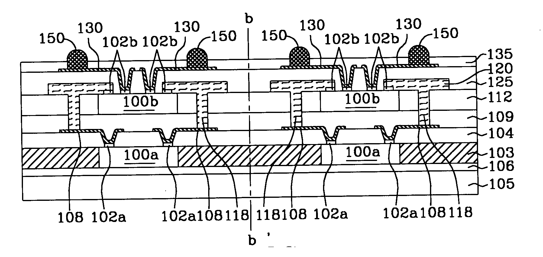
Figure 1 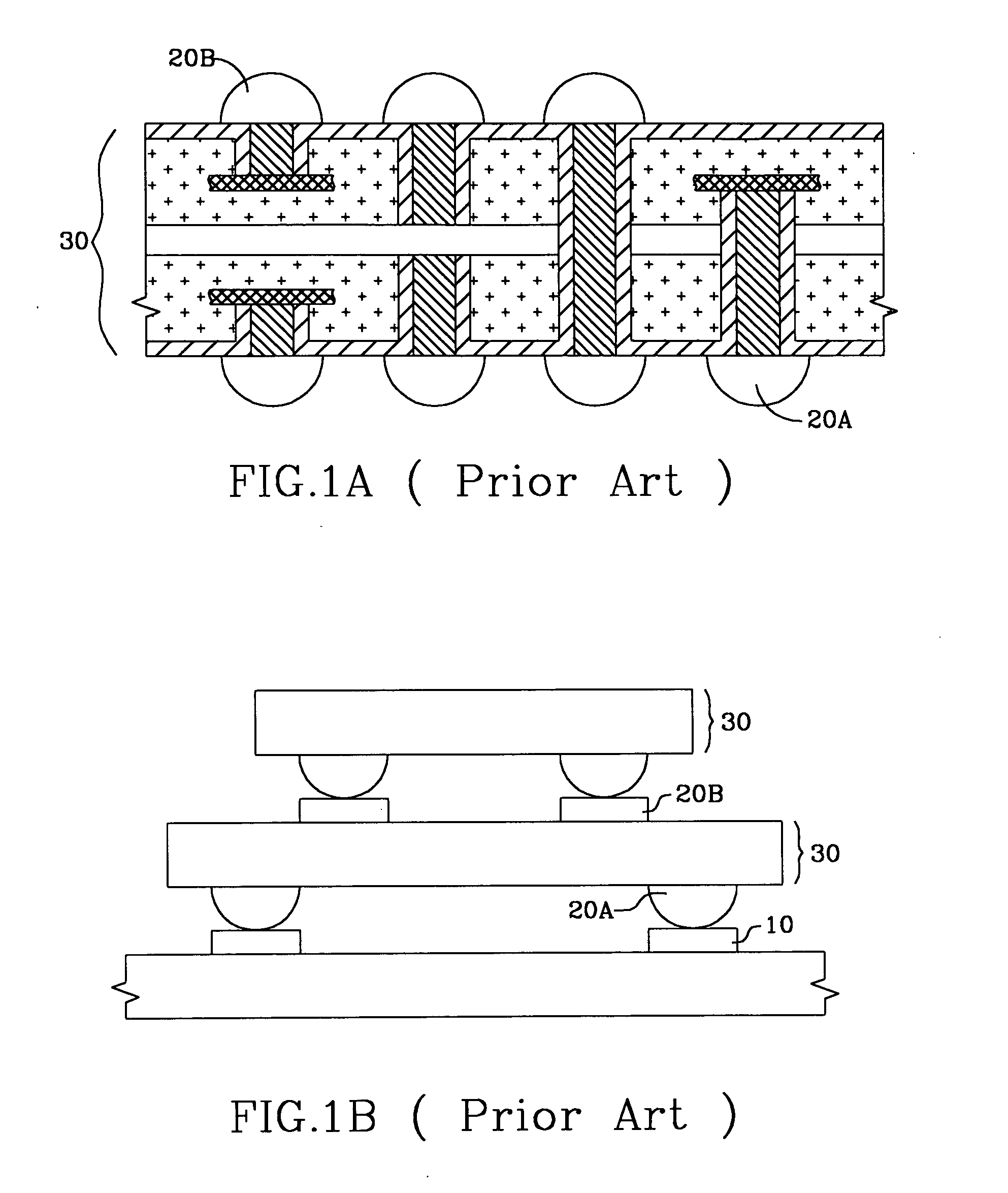
Figure 2 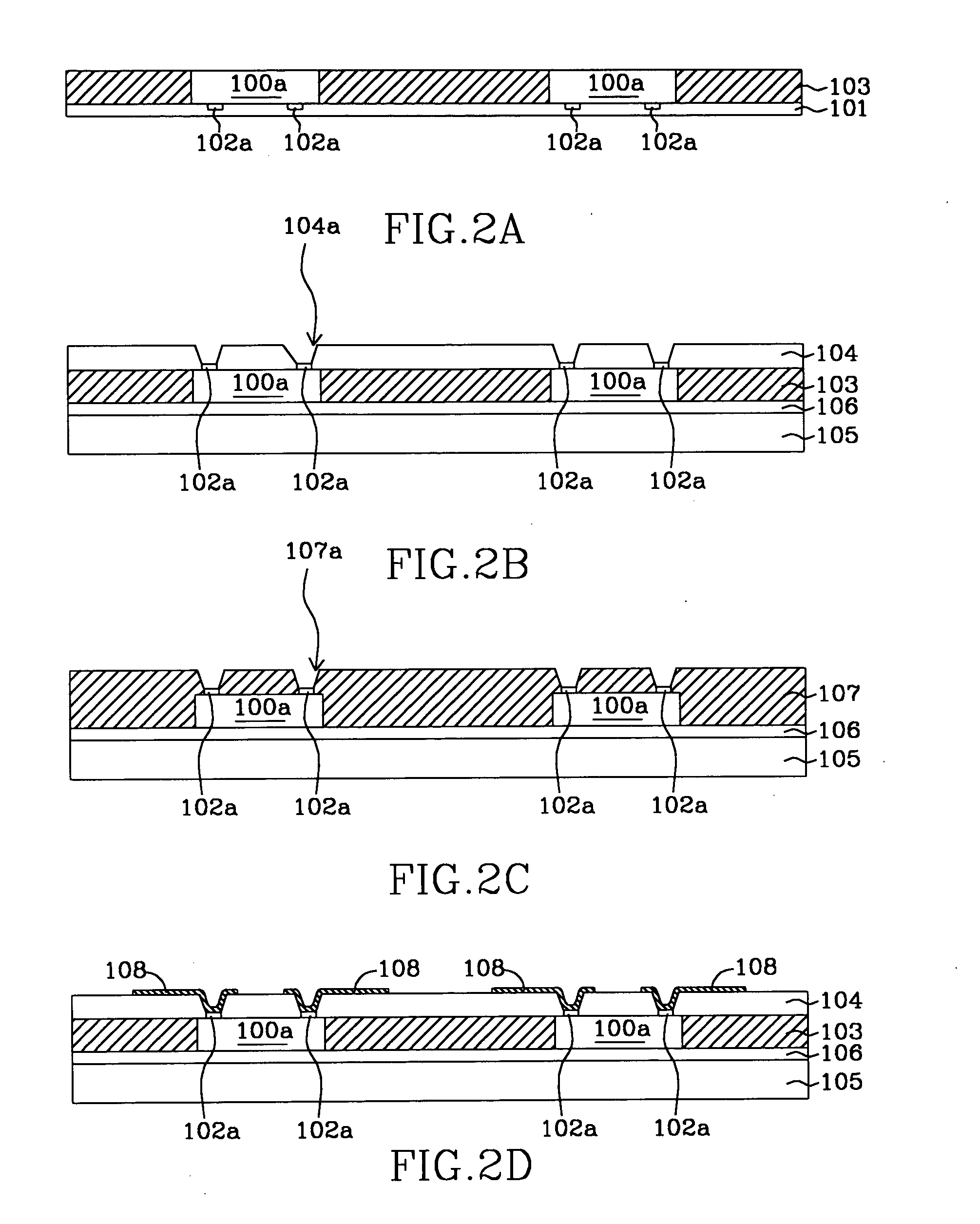
Figure 3
Abstract
Description
BACKGROUND OF THE INVENTION
[0001] 1. Field of Invention
[0002] This invention relates to a semiconductor assembly package. More particularly, the present invention is related to a multi-chips bumpless assembly package and a manufacturing method thereof.
[0003] 2. Related Art
[0004] Integrated circuits (chip) packaging technology is becoming a limiting factor for the development in packaged integrated circuits of higher performance. Semiconductor package designers are struggling to keep pace with the increase in pin count, size limitations, low profile, and other evolving requirements for packaging and mounting integrated circuits.
[0005] Originally, the electrical connections between the chips comprise wire bonding connection and flip chip connection. In wire bonding connection, a wire bonder is disposed above the first chip and then the tip of the conductive wire is melting to shape into a ball. Next, the conductive wire is bonded onto the bonding pad of the first chip. Then, the ...
Examples
Embodiment Construction
[0019] The multi-chips bumpless assembly package according to the preferred embodiments of this invention will be described herein below with reference to the accompanying drawings, wherein the same reference numbers refer to the same elements.
[0020]FIGS. 2A to 2G are partially enlarged cross-sectional views showing the progression of steps for forming a multi-chips bumpless assembly package according to the first preferred embodiment of this invention.
[0021] As shown in FIG. 2A, a plurality of first chips 100a with a plurality of first bonding pads 102a formed on a first active surfaces are placed on a first protection film 101 through attaching the first bonding pads 102a to the film 101. Therein, the first chips 100a are separated from each other to form a plurality of first gaps. Next, a first encapsulation 103 is provided to be filled in the first gaps so as to encompass the first chips 100a. To be noted, the first encapsulation 103 can be made of dielectric materials. Then, ...