
Si photodiode with symmetry layout and deep well bias in CMOS technology
Patent Information
- Authority / Receiving Office
- US · United States
- Current Assignee / Owner
- Publication Date
- 2012-07-12
- Estimated Expiration
- Not applicable · inactive patent
Smart Images
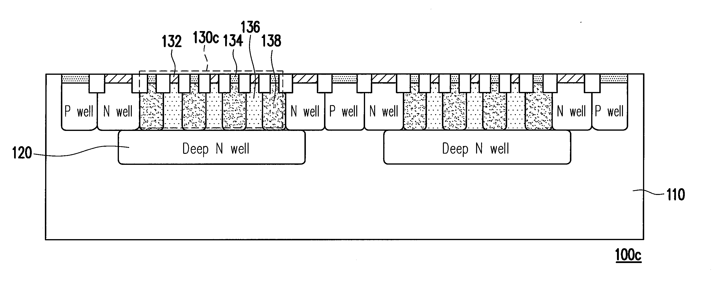
Figure 1 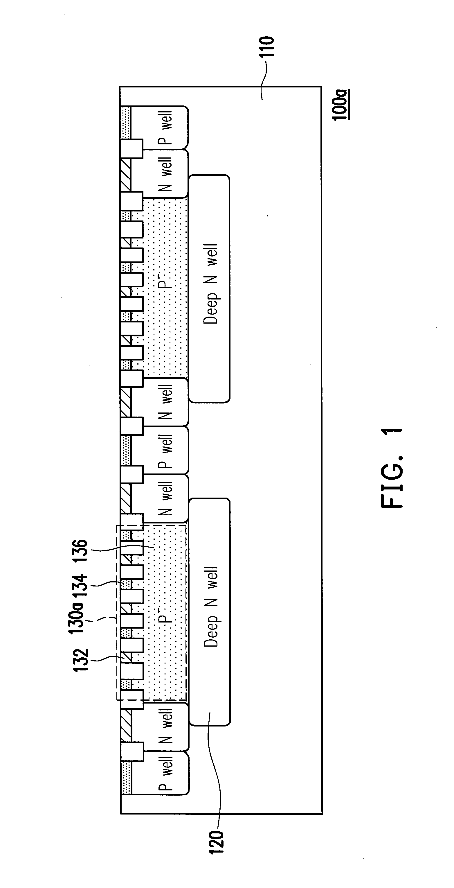
Figure 2 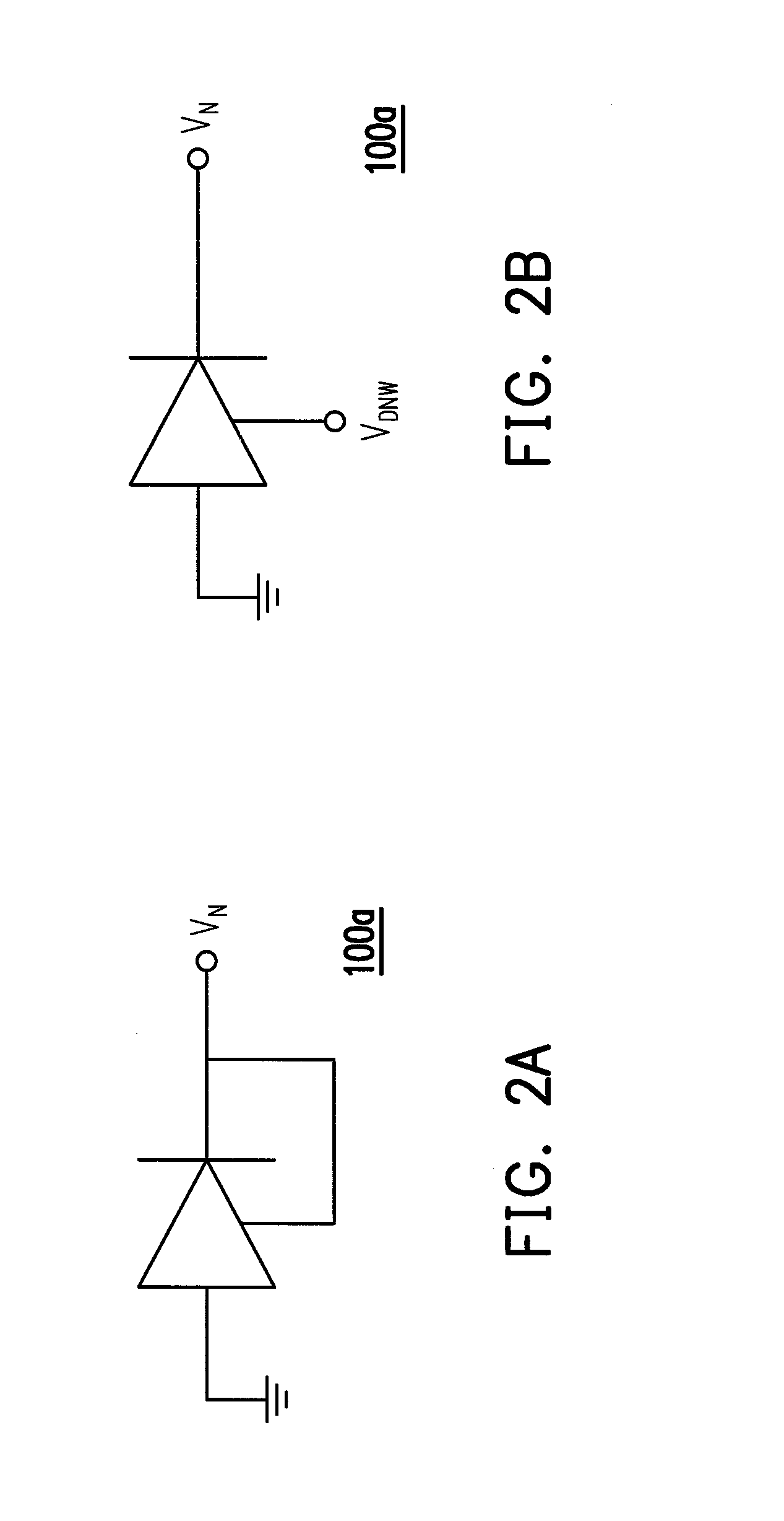
Figure 3
Abstract
Description
CROSS-REFERENCE TO RELATED APPLICATION
[0001] This application claims the priority benefit of Taiwan application serial no. 100100499, filed Jan. 6, 2011. The entirety of the above-mentioned patent application is hereby incorporated by reference herein and made a part of this specification.BACKGROUND OF THE INVENTION
[0002] 1. Field of the Invention
[0003] The invention relates to a photodiode and more particularly to a silicon photodiode with symmetry layout and deep well bias in CMOS technology.
[0004] 2. Description of Related Art
[0005] Nowadays, Si photodiodes (PDs) fabricated by complementary metal-oxide-semiconductor (CMOS) become popular in the application of optical communication at near-infrared wavelengths (e.g. 850-nm) due to its low cost and possible integration with receivers. However, light penetration depth of Si at 850-nm is larger than 10 μm that results in low responsivity for a surface PD. Moreover, carriers generated from bulk silicon substrate slowly diffuse to be collec...
Examples
Embodiment Construction
[0028]Silicon photodiodes are one of the most important devices in optical communication and are responsible for converting optical signals into electrical signals. However, when the material of a lower substrate of a silicon photodiode absorbs the absorption wavelengths of the silicon photodiode, the slow diffusion carriers from the substrate then becomes a problem which leads to slow response speed.
[0029]In an exemplary embodiment of the invention, the silicon photodiode adopts a deep well fabrication step and eliminates the effects and interferences generated after the substrate absorbs light by providing an extra deep well bias, such that the response speed and the frequency bandwidth are greatly improved. Moreover, in an exemplary embodiment of the invention, the silicon photodiode has a symmetrical surrounding structure for obtaining uniform electric field distribution. The interference from the noise of the substrate of the silicon photodiode is also reduced effectively.
[0030...