
Sigma-delta modulator
Patent Information
- Authority / Receiving Office
- US · United States
- Current Assignee / Owner
- Publication Date
- 2012-12-27
Smart Images
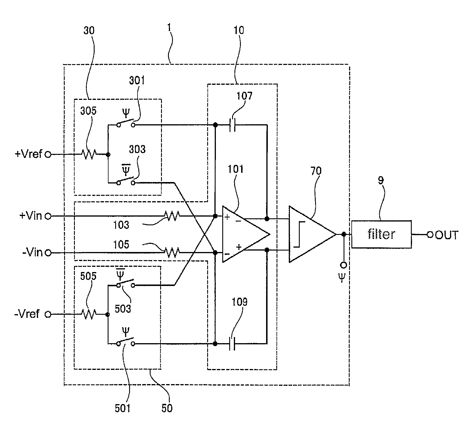
Figure 1 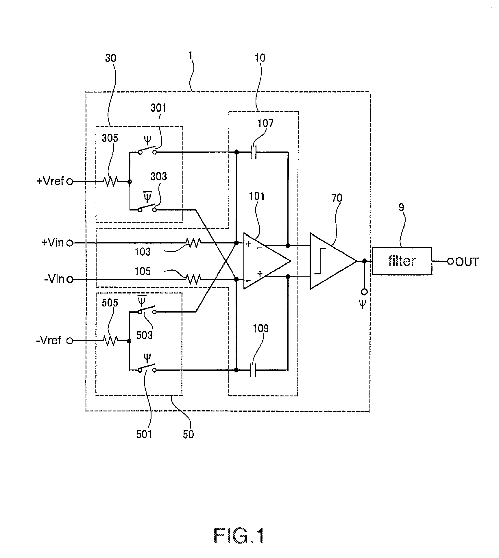
Figure 2 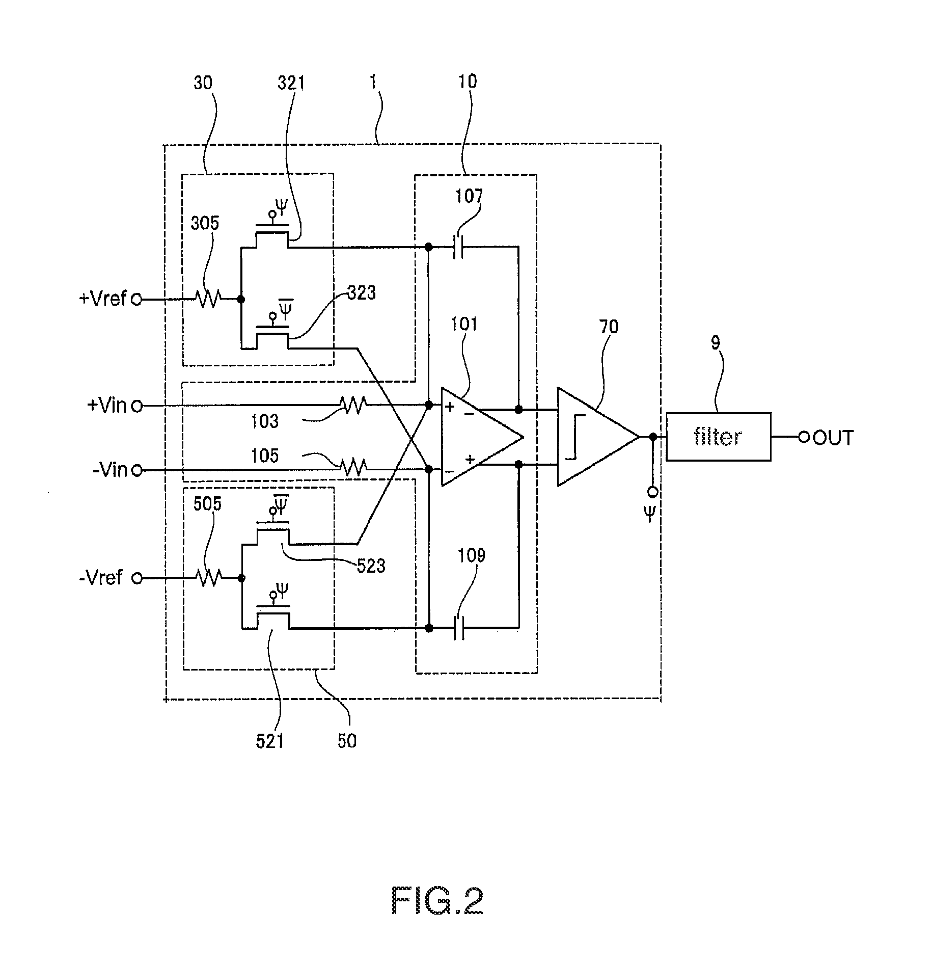
Figure 3
Abstract
Description
FIELD OF THE INVENTION
[0001] The present invention relates to a sigma-delta modulator. In particular, the sigma-delta modulator according to the present invention can be suitably used for, for example, an analog-to-digital (A / D) converter that converts analog signals into digital signals. Furthermore, the present invention also relates to a digital-to-analog (D / A) converter that is used in the sigma-delta modulator.BACKGROUND OF THE INVENTION
[0002] A / D converters have the function of converting analog data output by a sensor or the like into digital data. For this reason, such an A / D converter functions as an interface between a physical phenomenon and a digital circuit. A / D converters are widely used in a variety of fields such as the communication, medical and measurement fields, and are applied to radio devices such as mobile phones and television sets, medical instruments, health instruments, and measuring instruments.
[0003] The use of a sigma-delta modulator as a component of an A...
Examples
embodiment 1
[0030]FIG. 1 is a circuit diagram of an A / D converter that is configured using a sigma-delta modulator according to a first embodiment of the present invention. The MD converter shown in FIG. 1 includes a sigma-delta modulator 1 and a filter 9.
[0031]The sigma-delta modulator 1 integrates a first reference voltage +Vref and a second reference voltage −Vref, whose polarities are controlled using a digital signal Ψ, and input voltages +Vin and −Vin, quantizes them, and then outputs a binary (or multinary) digital signal Ψ. The sigma-delta modulator 1 includes an integration circuit 10, a comparator 70, a first DAC unit 30, and a second DAC unit 50.
[0032]The integration circuit 10 includes a fully differential amplifier 101, a first capacitor 107, a second capacitor 109, a first input resistor 103, and a second input resistor 105.
[0033]The fully differential amplifier 101 includes a non-inverted input terminal and an inverted input terminal as input terminals, and an inverted output ter...
first embodiment
Variant of First Embodiment
[0053]FIG. 2 is a circuit diagram of an A / D converter that is configured using the sigma-delta modulator of FIG. 1 according to a variant of the first embodiment. In FIG. 2, the first switch 301, the second switch 303, the third switch 501, and the fourth switch 503 shown in FIG. 1 are implemented using a transistor 321, a transistor 323, a transistor 521, and a transistor 523, respectively.
[0054]It is preferable to use nMOSs as the transistor 321, the transistor 323, the transistor 521, and the transistor 523 (however, there are cases where pMOSs are preferable depending on the level of electric potential). Since the switches are formed of nMOSs, the ON resistances of the switches are reduced, so that the size of the switches can be made smaller. Furthermore, since the switches are smaller, the influence of the parasitic capacitance decreases, so that feedthrough or charge injection (a parameter related to an analog switch; when an analog switch is turned...
second embodiment
[0060]FIG. 3 is a circuit diagram of an A / D converter that is configured using a sigma-delta modulator according to a second embodiment of the present invention. The A / D converter shown in FIG. 3 includes a sigma-delta modulator 3 and a filter 9.
[0061]The sigma-delta modulator 3 integrates voltages obtained using reference voltages +Vref and −Vref and input voltages +Vin and −Vin, and then outputs digital signals. The sigma-delta modulator 3 includes an integration circuit 10 and a DAC unit 40. Furthermore, the DAC unit 40 includes a first DAC unit and a second DAC unit.
[0062]Here, first to fourth voltages are defined as follows. When the first reference voltage +Vref is supplied to one end of a first resistor 413, voltage obtained at the other end thereof is defined as the first voltage. When the second reference voltage −Vref is supplied to one end of a second resistor 417, voltage obtained at the other end thereof is defined as the second voltage. When the second reference voltag...