

Integrated circuit product yield optimization using the results of performance path testing
Patent Information
- Authority / Receiving Office
- US · United States
- Current Assignee / Owner
- Publication Date
- 2014-02-13
- Estimated Expiration
- Not applicable · inactive patent
Smart Images
Figure 1 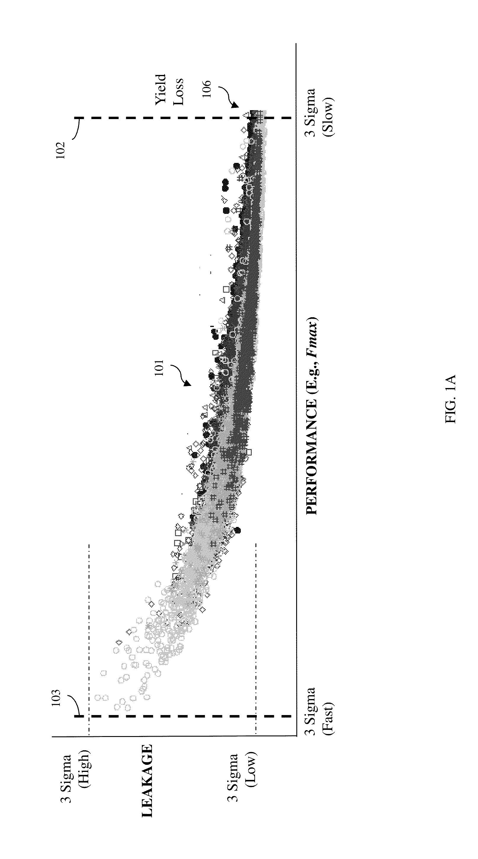
Figure 2 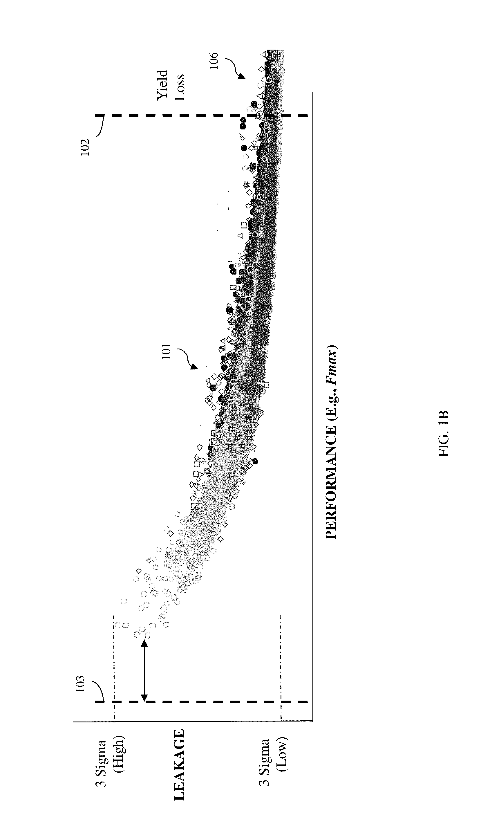
Figure 3
Abstract
Description
BACKGROUND
[0001] 1. Field of the Invention
[0002] The embodiments disclosed herein relate to integrated circuit product yield and, more particularly, to a method, system and computer program product for optimizing integrated circuit product yield based on the results of post-manufacture performance path testing.
[0003] 2. Description of the Related Art
[0004] Currently, performance measurements and, particularly, frequency measurements acquired during performance screen ring oscillator (PSRO) testing are often used to disposition (i.e., screen) chips at both the wafer-level and the module-level (i.e., the integrated circuit chip package-level). For purposes of this disclosure, wafer-level chip dispositioning refers to wafer-level performance testing to determine whether chips on wafers pass and, thus, are processed into chip modules or fail and, thus, are scrapped. Similarly, module-level chip dispositioning refers to module-level performance testing to determine whether the chip modules p...
Examples
Embodiment Construction
[0020]As mentioned above, currently, performance measurements and, particularly, frequency measurements acquired during performance screen ring oscillator (PSRO) testing are often used to disposition (i.e., screen) chips at both the wafer-level and the module-level (i.e., the integrated circuit chip package-level). For purposes of this disclosure, wafer-level chip dispositioning refers to wafer-level performance testing to determine whether the chips on wafers pass and, thus, are processed into chip modules or fail and, thus, are scrapped. Similarly, module-level chip dispositioning refers to module-level performance testing to determine whether the chip modules pass and, thus, are shipped to customers or fail and, thus, are scrapped. Performance measurements acquired during post-manufacture (i.e., wafer-level or module-level) PSRO testing are also often used as feedback to control or re-center (i.e., re-calibrate) the manufacturing line in order to account for product-to-product la...