
Sige source/drain structure and preparation method thereof
Patent Information
- Authority / Receiving Office
- US · United States
- Current Assignee / Owner
- Publication Date
- 2018-06-07
Smart Images
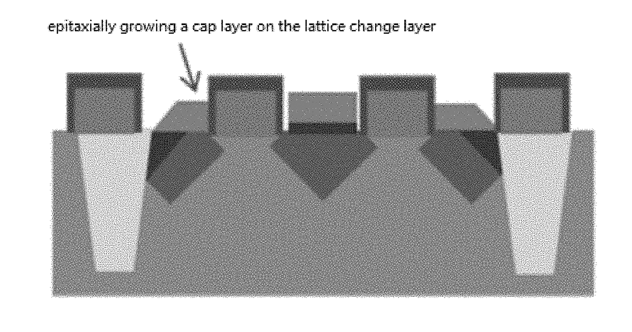
Figure 1 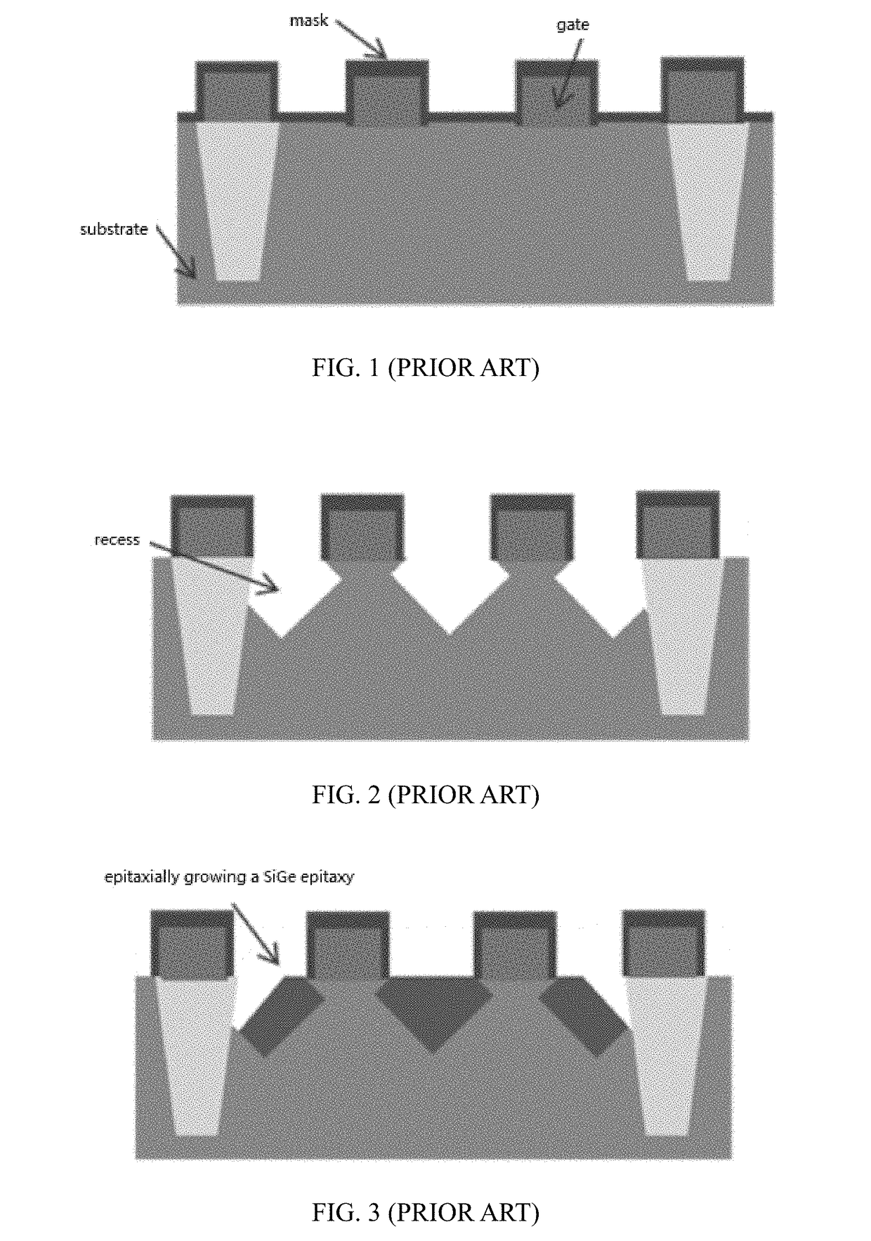
Figure 2 
Figure 3
Abstract
Description
CROSS-REFERENCE TO RELATED APPLICATION
[0001] This application claims the priority benefit of China patent application serial No. 201611093086.2, filed Dec. 1, 2016. The entire contents of the above-mentioned patent application are hereby incorporated by reference herein and made a part of the specifications.FIELD OF THE INVENTION
[0002] The present invention relates to semiconductor silicon wafer process in the field of IC manufacturing technology, and particularly to a structure and preparation of SiGe source / drain.BACKGROUND OF THE INVENTION
[0003] With the development of the IC manufacturing technology, the size of field effect transistor (FET) has been reducing. So, strain technology has been introduced to change lattice structure of channel for improving the carrier mobility in a channel. It has been known from the existing studies that the application of tensile stress in the channel can increase the electron mobility, while the application of compressive stress can increase the ho...
Examples
Embodiment Construction
[0050]The present invention will be described in further details hereinafter by referring to the accompanying drawings, so as to provide a better understanding of the present invention.
[0051]It should be noted that, in the following specific embodiments, when these embodiments of the present invention are described in detail, in order to clearly illustrate the structure of the present invention to facilitate explanation, the accompanying drawings are not necessarily drawn to scale, some features in the drawings may have been fragmentary enlarged, deformed or simplified. Therefore, it should be avoided to understand this as a limitation to the present invention.
[0052]Compared with the prior art, the same with the prior art, structure of SiGe source / drain of the present invention comprises a semiconductor single crystal silicon substrate, a SiGe seed layer and a SiGe bulk layer, and a cap layer. Wherein, the semiconductor single crystal silicon substrate has a prepared gate and two re...