
Planar orthomode transducer
a transducer and orthomode technology, applied in the field of microwave devices, can solve the problems of large dimensions, high manufacturing cost, and difficulty in integrating such waveguide orthomode transducers into the microwave front-end of the transceiver device, and achieve the effects of improving polarization diversity, widening the operating frequency band, and reducing insertion losses
Patent Information
- Authority / Receiving Office
- US · United States
- Patent Type
- Applications(United States)
- Current Assignee / Owner
- Publication Date
- 2019-06-20
Smart Images
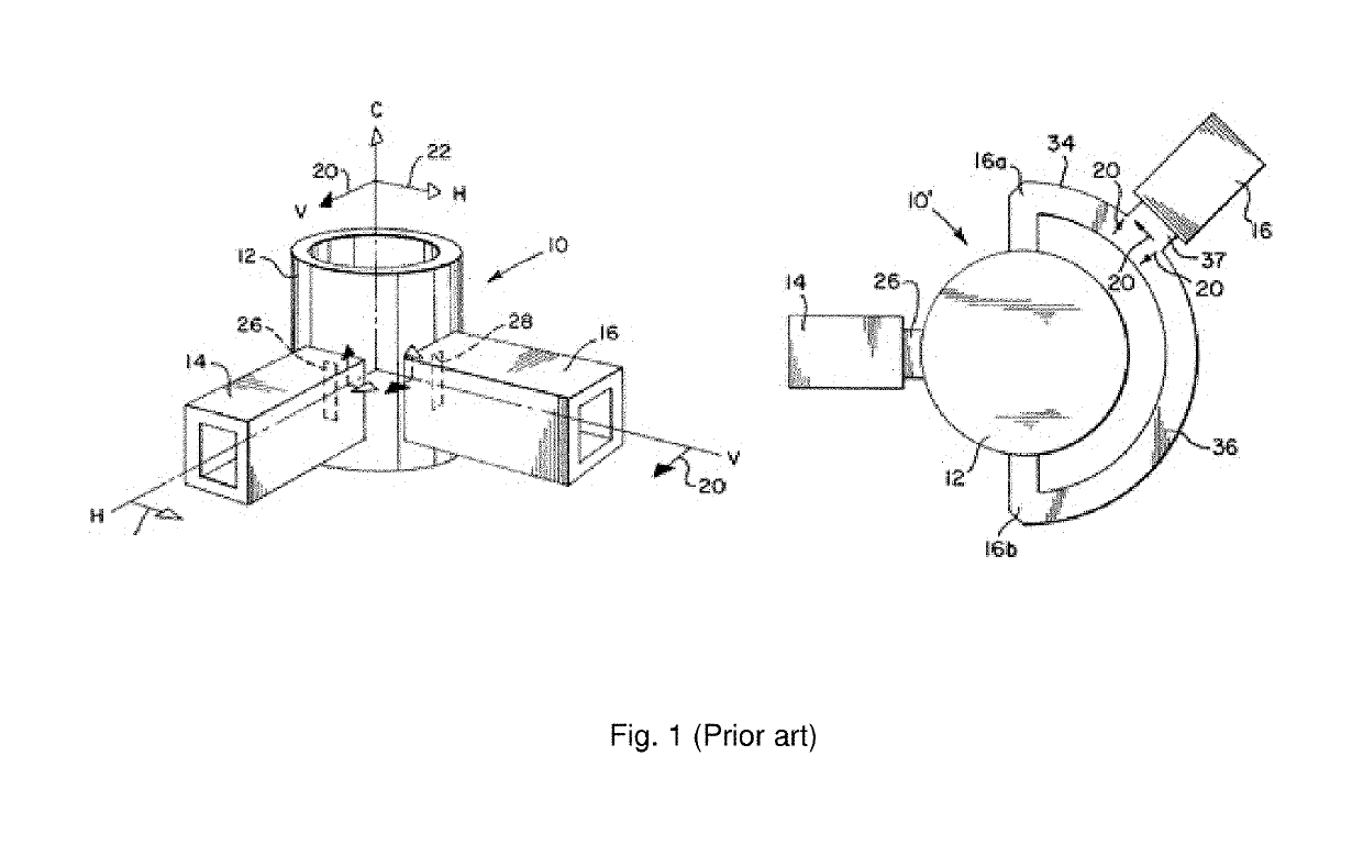
Figure 1 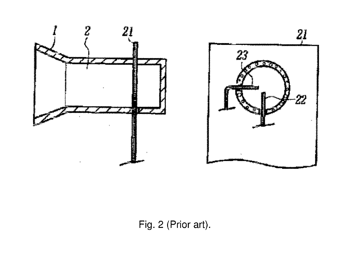
Figure 2 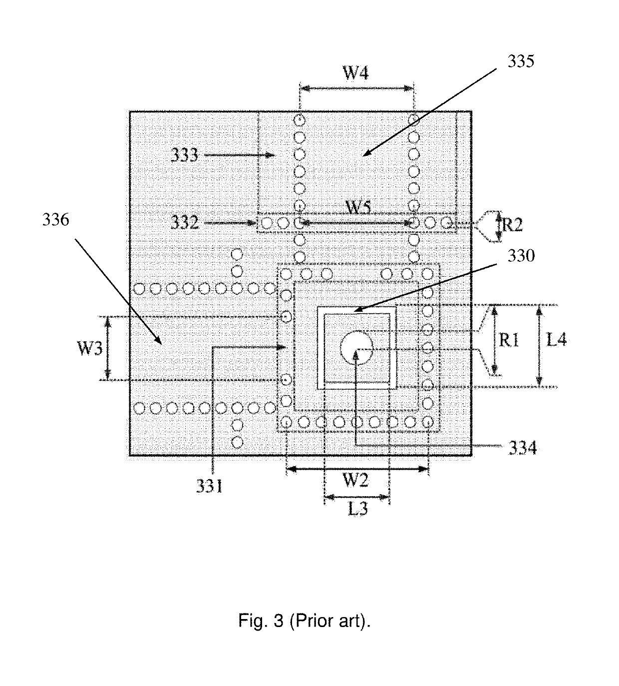
Figure 3
Abstract
Description
FIELD OF THE INVENTION
[0001] The present invention relates to the field of microwave devices and more specifically to splitters or combiners of electromagnetic waves with orthogonal polarizations.BACKGROUND OF THE INVENTION
[0002] One of the methods to increase a wireless communication system throughput is the usage of two orthogonal polarizations than can be done without significant sophistication of the transceiver. This enables a simultaneous transmission and / or receipt of two data flows, each flow being carried by orthogonally polarized electromagnetic waves. The key components of such a system are dual polarized antennas and orthomode transducers, which are devices used to distinguish appropriately polarized waves from the common dual-pol antenna port. Each of single-pol waves is guided to one or more orthomode transducers ports.
[0003] Traditionally, orthomode transducers are provided on hollow metallic waveguides, and more specifically on several waveguides of rectangular cross-se...
Examples
Embodiment Construction
[0046]One embodiment of the present invention of a planar orthomode transducer is shown in FIG. 4. It comprises a substrate integrated resonator (1) with two substrate integrated waveguides (2) connected to the substrate integrated resonator (1), wherein the substrate integrated resonator (1) and the substrate integrated waveguides (2) are formed by a plurality of metallized via holes between two metallization layers of a printed circuit board (10). The substrate integrated waveguide (2) is shown in FIG. 5. Metallized via holes connecting bottom and top metallization layers of the printed circuit board (10) form sidewalls of the substrate integrated waveguides (2). Top and bottom metallization layers of the printed circuit board (10) form top and bottom walls of the substrate integrated waveguides (2). Thus, substrate integrated waveguides (2) have dielectric filling that consists of the printed circuit board (10) substrate material. Operating principle of the substrate integrated w...