
Semiconductor substrate with trenches for reducing substrate resistance
Patent Information
- Authority / Receiving Office
- US · United States
- Current Assignee / Owner
- Publication Date
- 2005-02-22
- Estimated Expiration
- Not applicable · inactive patent
Smart Images
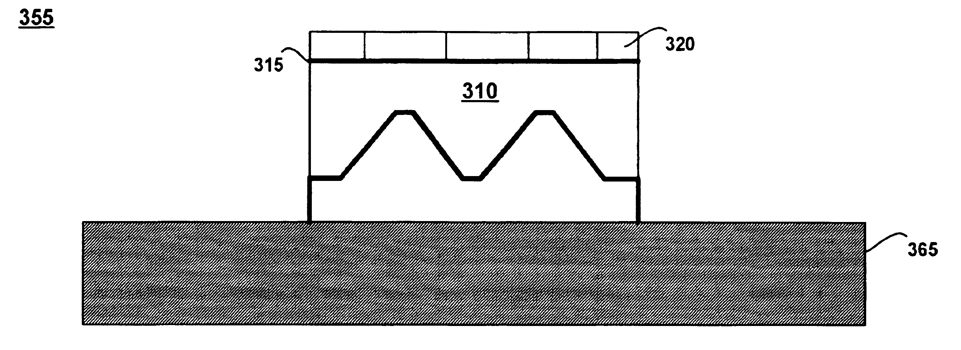
Figure 1 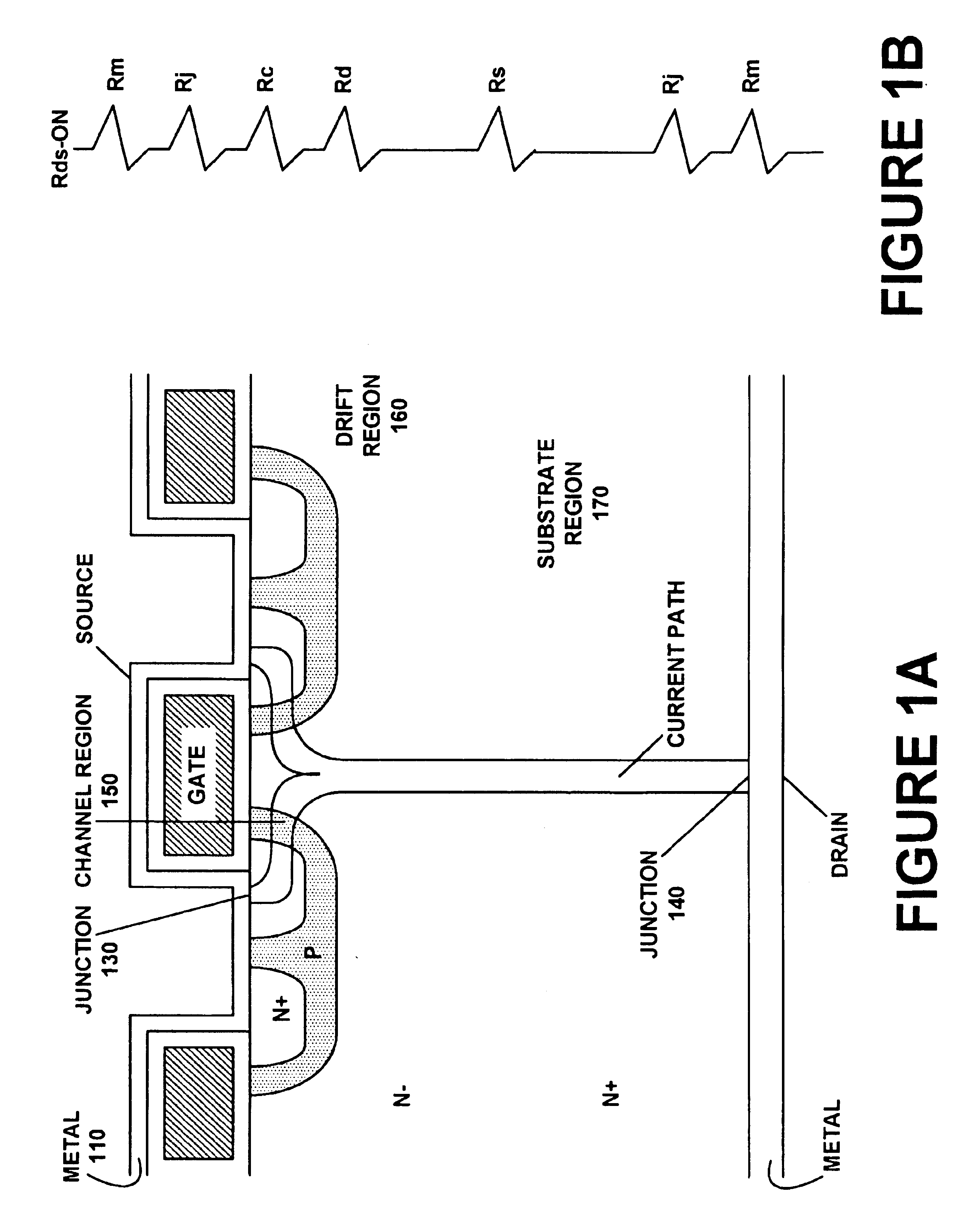
Figure 2 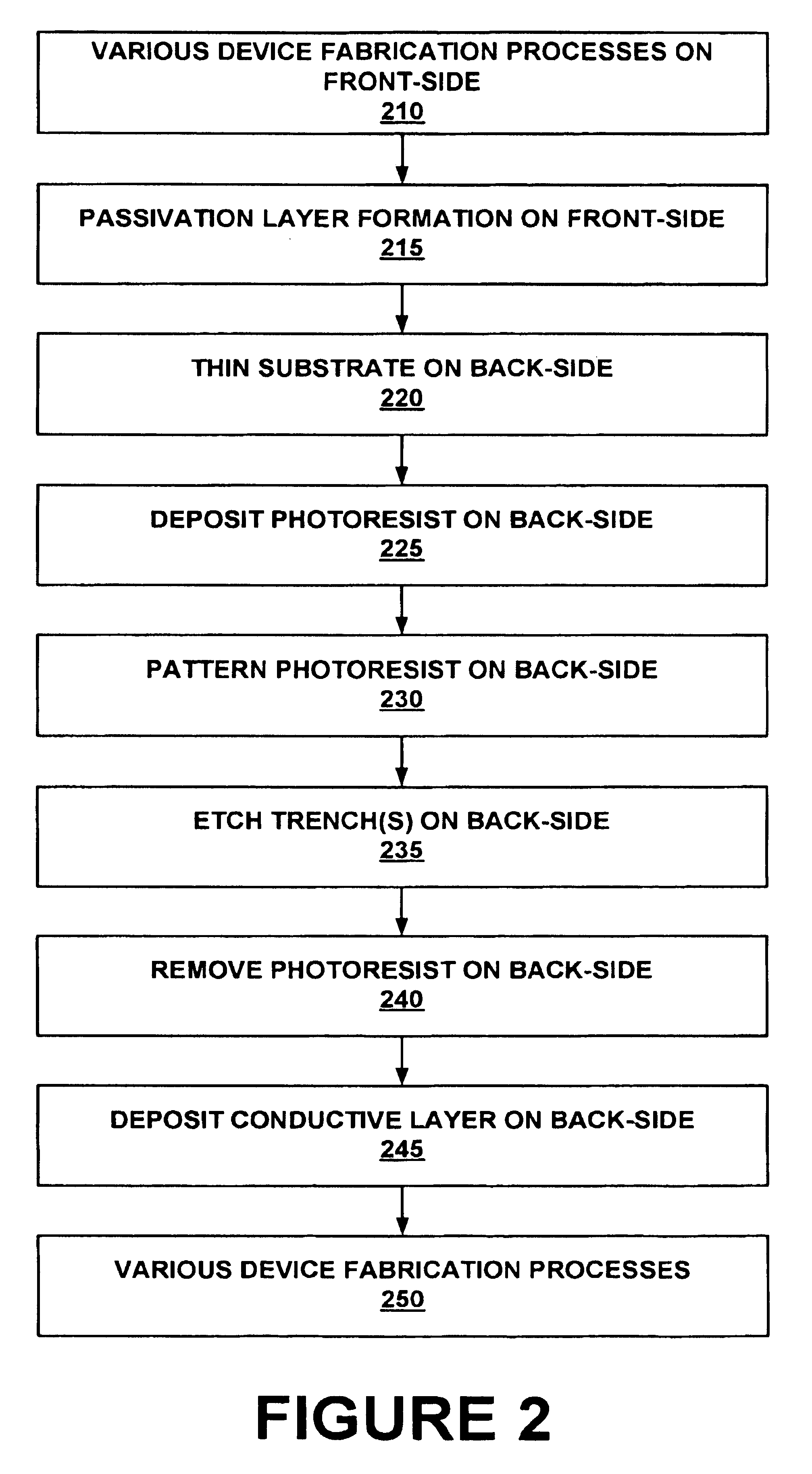
Figure 3
Abstract
Description
FIELD OF THE INVENTIONEmbodiments of the present invention relate to semiconductor device fabrication, and more particularly to reduced substrate resistance characteristics.BACKGROUND OF THE INVENTIONFor power metal oxide semiconductor field effect transistors (MOSFET), substrate resistance contributes to the total on-state resistance as a parasitic component. A vertical semiconductor device like a vertical double-diffused MOSFET (VDMOSFET), a trench MOSFET (TMOSFET), an insulated gate bipolar transistor (IGBT), or the like, represent a power switch. The resistance in the on-state of the switch is composed of a series connection of resistive elements.FIG. 1A shows a cross sectional view of an VDMOSFET device employed in the conventional art. While FIG. 1B shows a corresponding series connection of resistive elements modeling the conductive path in the device in the on-state employed in the conventional art. The on-state resistance (Rds-on) comprises metal film resistance (Rm) 110, 1...
Examples
Embodiment Construction
Reference will now be made in detail to the embodiments of the invention, examples of which are illustrated in the accompanying drawings. While the invention will be described in conjunction with the preferred embodiments, it will be understood that they are not intended to limit the invention to these embodiments. On the contrary, the invention is intended to cover alternatives, modifications and equivalents, which may be included within the spirit and scope of the invention as defined by the appended claims. Furthermore, in the following detailed description of the present invention, numerous specific details are set forth in order to provide a thorough understanding of the present invention. However, it will be obvious to one of ordinary skill in the art that the present invention may be practiced without these specific details. In other instances, well-known methods, procedures, components, and circuits have not been described in detail as not to unnecessarily obscure aspects of...