
Trench MOSFET with on-resistance reduction
a technology of mosfet and drain, which is applied in the field of cell structure and fabrication process of power semiconductor devices, can solve the problems of poor metal coverage, unreliable electrical contact, and difficulty, and achieve the effect of reducing drain and source resistance, shortening p-body anneal or diffusion, and reducing drain-source resistan
Patent Information
- Authority / Receiving Office
- US · United States
- Patent Type
- Applications(United States)
- Current Assignee / Owner
- Publication Date
- 2011-01-13
- Estimated Expiration
- Not applicable · inactive patent
Smart Images
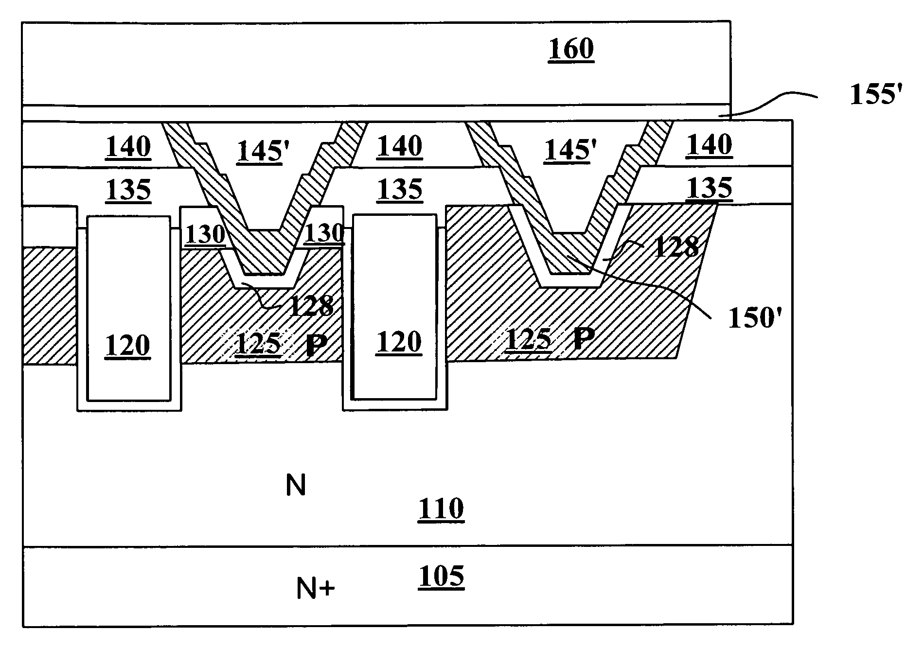
Figure 1 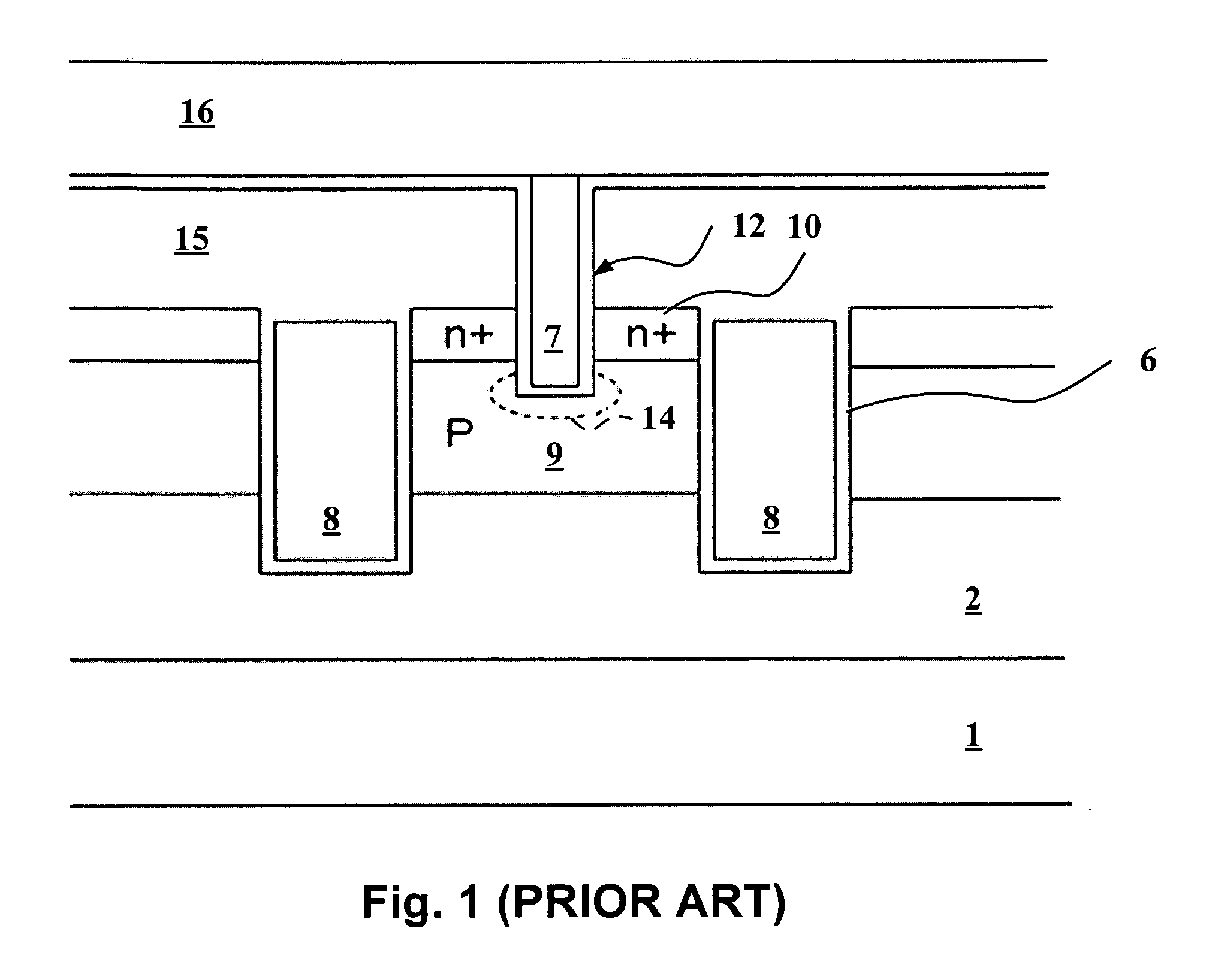
Figure 2 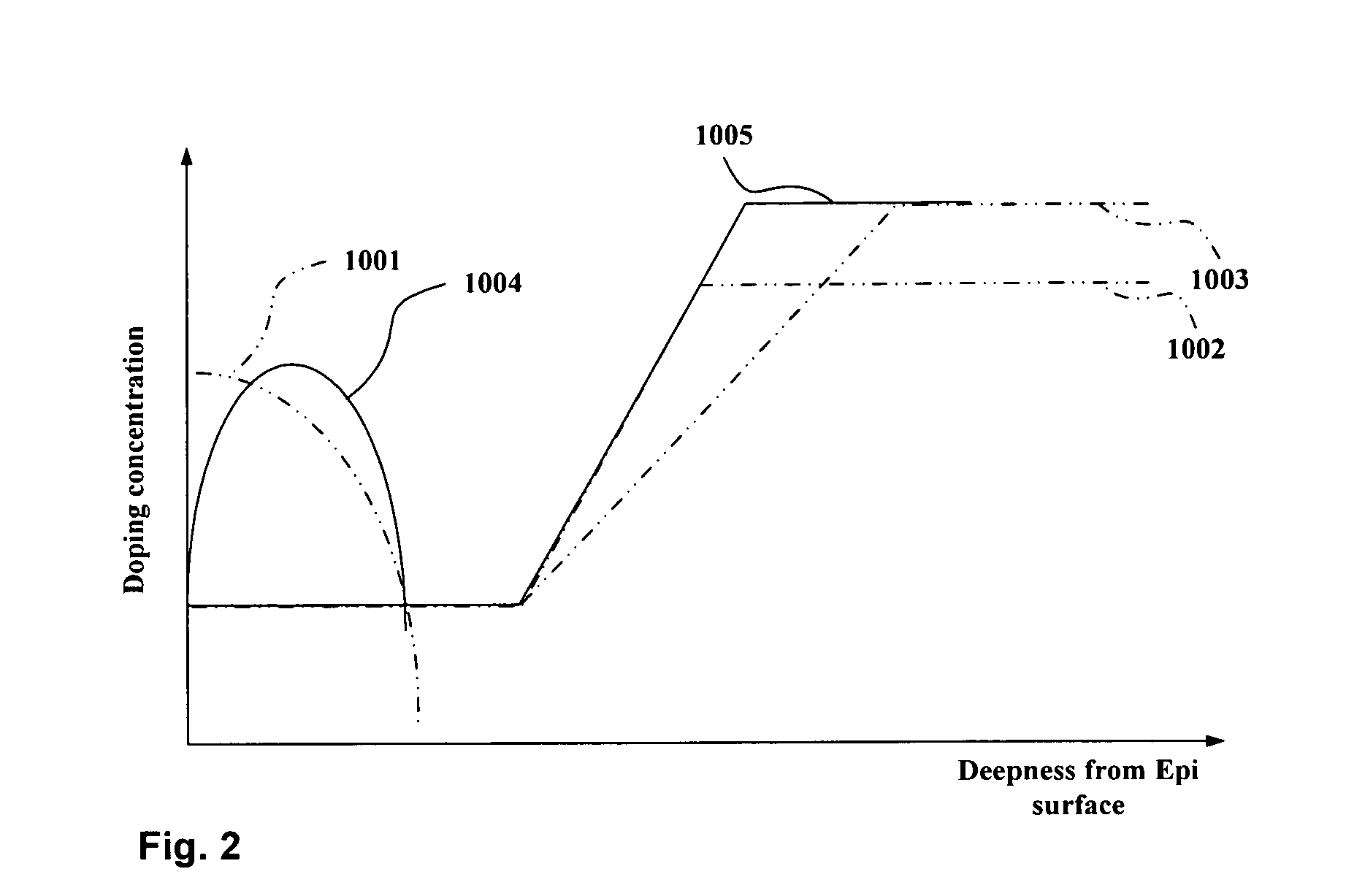
Figure 3
Abstract
Description
BACKGROUND OF THE INVENTION
[0001] 1. Field of the Invention
[0002] This invention relates generally to the cell structure and fabrication process of power semiconductor devices. More particularly, this invention relates to a novel and improved cell structure and improved process of fabricating a trenched semiconductor power device with reduced drain-source resistance and better metal step coverage.
[0003] 2. The Prior Arts
[0004] Conventional technologies of forming aluminum metal contact to the N+ source and P-well formed in the P-body regions in a semiconductor device is encountering a technical difficulty of poor metal coverage and unreliable electrical contact when the cell pitch is shrunken. The technical difficulty is especially pronounced when a metal oxide semiconductor field effect transistor (MOSFET) cell density is increased above 200 million cells per square inch (200 M / in2) with the cell pitch reduced to 1.8 um or to even a smaller dimension. The metal contact space to both N+...
Examples
Embodiment Construction
[0023]Please refer to FIG. 3 for preferred an embodiment of this invention where a metal oxide semiconductor field effect transistor (MOSFET) device 100 is formed on a Phosphorus N+ substrate 105 formed with an N epitaxial layer 110. The MOSFET 100 includes a trenched gate 120 disposed in a trench with a gate insulation layer formed over the walls of the trench. A body region 125 that is doped with a dopant of second conductivity type, e.g., P-type dopant, extends between the trenched gates 120.
[0024]For the purpose of reduce the drain-source resistance significantly, the substrate of this invention is Phosphorus substrate as mentioned which has a resistivity lower than 2.0 mohm-cm. On the other hand, P-body region is implemented by medium or high energy (100˜400 KeV) Ion Implantation and followed by Anneal at 1000˜1100 C to form a retrograded P-body / N-Epi junction (1004 in FIG. 2) with thinner Epi. And incorporated with the Phosphorus substrate (1005 in FIG. 2), the impact of drift...