
Semiconductor Device and Manufacturing Method Thereof
a semiconductor and manufacturing method technology, applied in the field of semiconductor elements, can solve the problems of difficult control of impurity concentration profiles, inability to simplify the manufacture of semiconductor elements, and breakage of elements, so as to reduce the series resistance of a substrate, increase the operating speed of an element, and facilitate the effect of obtaining
Patent Information
- Authority / Receiving Office
- US · United States
- Patent Type
- Applications(United States)
- Current Assignee / Owner
- Publication Date
- 2007-11-01
- Estimated Expiration
- Not applicable · inactive patent
Smart Images
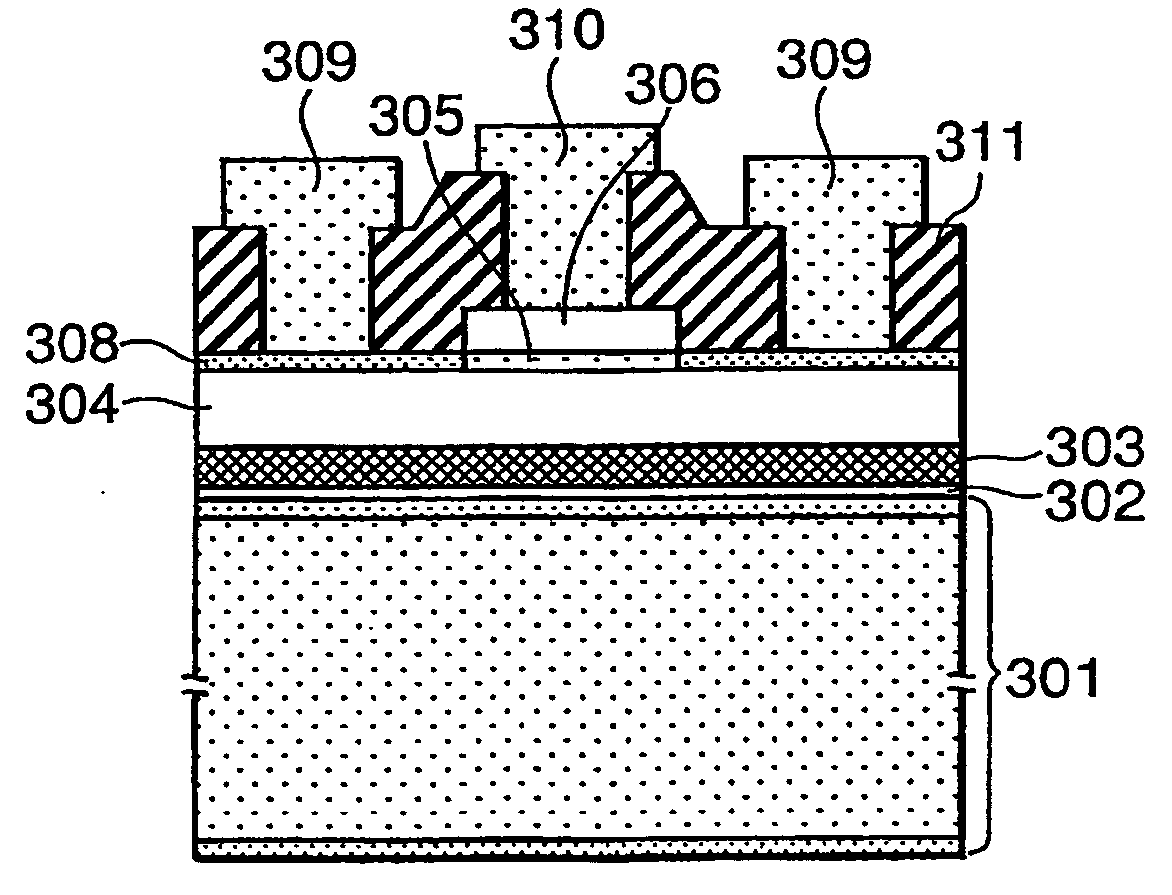
Figure 1 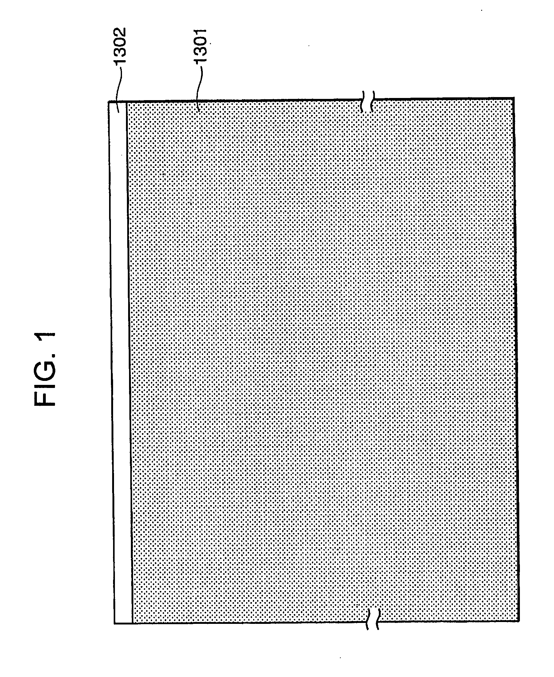
Figure 2 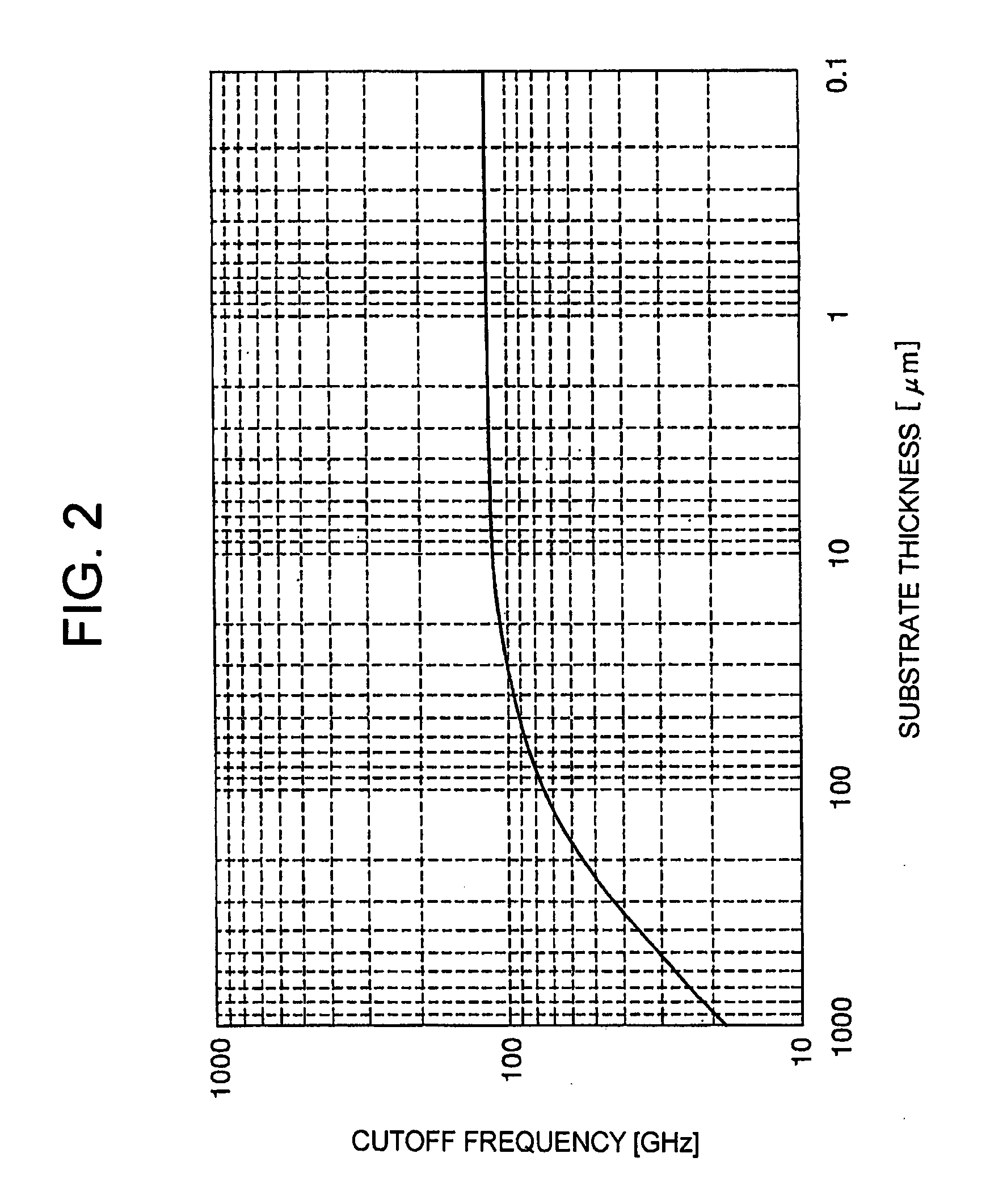
Figure 3
Abstract
Description
TECHNICAL FIELD
[0001] This invention relates to a semiconductor element that operates at high speed and high power, and a manufacturing method thereof. BACKGROUND ART
[0002] High-speed transistors adapted to operate in a microwave band and high-power transistors for use in power conversion are applied to various fields such as household electrical appliances.
[0003] As a semiconductor element forming a high-speed transistor or a high-power transistor, there is a bipolar transistor, a thyristor, a GTO, an IGBT, a MOSFET, or the like. Such an element is required to turn on / off the high power at high speed in response to a pulse signal and, thus, for the purpose of satisfying both supply voltage resistance and speediness, use has been made of a semiconductor substrate that differs from an integrated circuit substrate formed in a flat shape.
[0004] As the semiconductor substrate that has been used for forming such an element, use has been made, as shown in FIG. 1, of a two-layer struct...
Examples
embodiment 1
[0046] The structure and manufacturing method of a semiconductor substrate according to embodiment 1 of this invention will be described hereinbelow with reference to FIG. 3. A conductivity type referred to hereinbelow represents an n-type or a p-type of a silicon semiconductor and a change in impurity concentration is also included in a difference in conductivity type. FIG. 3 shows a sectional structure of a bipolar transistor substrate according to this embodiment. In FIG. 3, the bipolar transistor substrate comprises a Si layer 101 having a first conductivity type for forming an emitter layer, a Si layer 102 having a conductivity type opposite to the first conductivity type as a second conductivity type for forming a base layer, a Si layer 103 having a third conductivity type for forming a collector layer, a Si layer 104 having a fourth conductivity type for forming a collector electrode contact region, a metal substrate 108 connected to the Si layer having the fourth conductivit...
embodiment 2
[0064] The structure of a semiconductor substrate according to embodiment 2 of this invention will be described with reference to FIG. 6. FIG. 6 shows a vertical-type MOSFET substrate in this embodiment 2, wherein it comprises, on a metal substrate 401, a high-concentration drain layer 403 having a first conductivity type, a drain layer 404 having a second conductivity type which differs from the first conductivity type in impurity concentration, and a body layer 405 having a third conductivity type being a conductivity type opposite to the first conductivity type and used for forming a MOSFET channel. These layers are formed on a silicon substrate having a {110} plane by the same method as that shown in embodiment 1.
[0065] The conductivity types, impurity concentrations, and thicknesses of the respective layers are set to n-type, 1×1020 cm−3, and 0.2 μm for the high-concentration drain layer, n-type, 2×1017 cm−3, and 0.5 μm for the drain layer, and p-type, 5×1018 cm−3, and 0.2 μm ...
embodiment 3
[0086] The structure of a semiconductor substrate according to embodiment 3 of this invention will be described with reference to FIG. 8. FIG. 8 shows a vertical-type IGBT substrate in this embodiment 3, wherein it comprises, on a metal substrate 601, an anode layer 603 having a first conductivity type, a buffer layer 604 having a second conductivity type opposite to the first conductivity type, a conductivity modulation layer 605, and a gate layer 606 having a third conductivity with the same polarity as that of the anode layer. These layers are formed on a silicon substrate having a {110} plane by the same method as that shown in embodiment 1. In this embodiment, the conductivity types, impurity concentrations, and thicknesses of the respective layers are set to p-type, 1×1020 cm−3, and 0.2 μm for the anode layer, n-type, 1×1020 cm−3, and 0.2 μm for the buffer layer, n-type, 2×1017 cm−3, and 0.2 μm for the conductivity modulation layer, and p-type, 5×1018 cm−3, and 0.2 μm for the ...