
Liquid crystal display device
Patent Information
- Authority / Receiving Office
- US · United States
- Current Assignee / Owner
- Publication Date
- 2005-11-08
- Estimated Expiration
- Not applicable · inactive patent
Smart Images
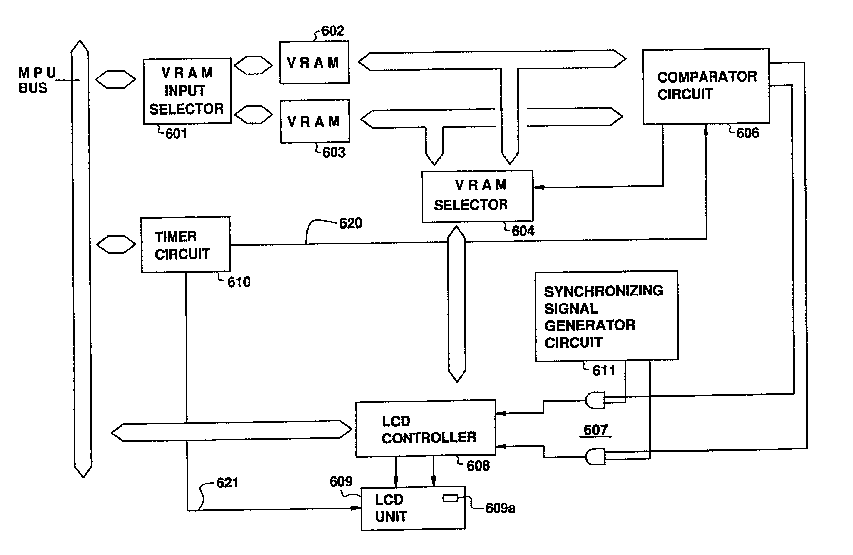
Figure 1 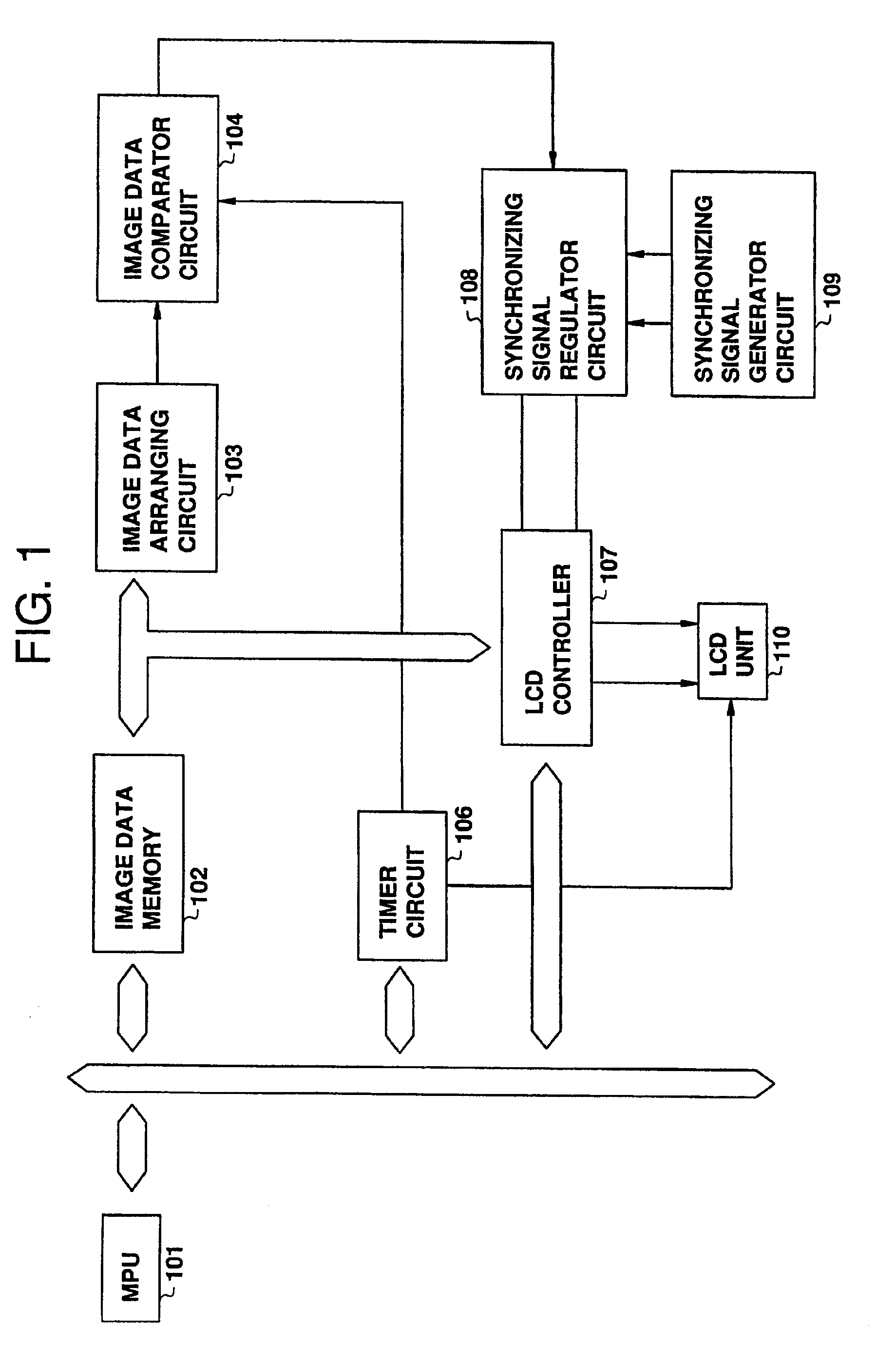
Figure 2 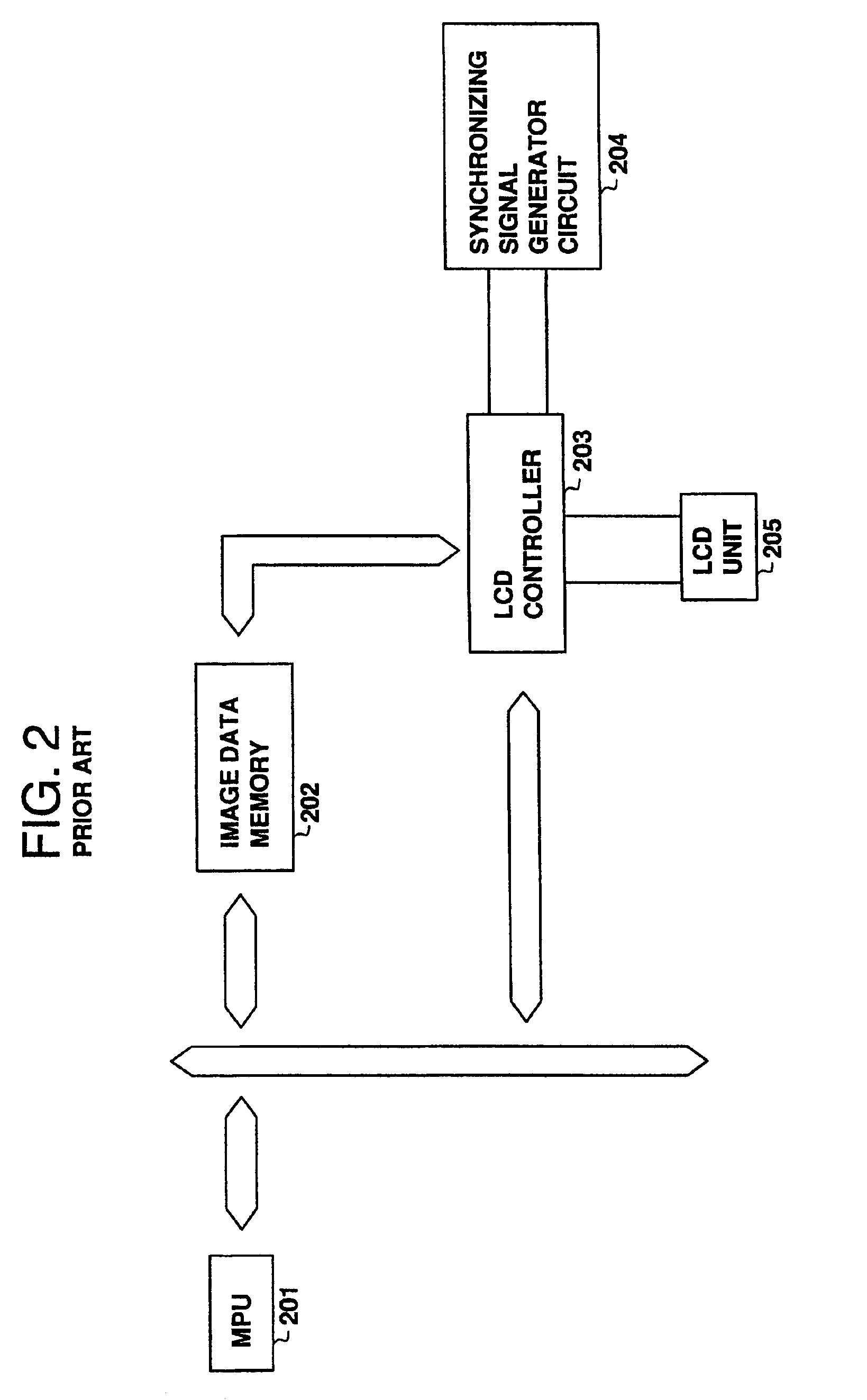
Figure 3
Abstract
Description
[0001] This is a division of U.S. application Ser. No. 09 / 010,482, filed 21 Jan. 1998, now U.S. Pat. No. 6,380,932, which is a division of U.S. application Ser. No. 08 / 447,932, filed 23 May 1995, now U.S. Pat. No. 5,812,149.BACKGROUND OF THE INVENTION
[0002] The present invention relates to a liquid crystal display device capable of reducing a consumption power.
[0003] As shown in FIG. 2, a liquid crystal display (LCD) controller 203 is connected with an LCD unit 205, an image data memory 202, a micro-processing unit (MPU) 201 and a synchronizing signal generator circuit 204. Under commands of MPU 201, image data stored in the image data memory 202 is input to the LCD controller 203 and is signal-converted, so that the converted image data is displayed on the LCD unit 205.
[0004] In a conventional LCD controller, when the same (frame) image data is displayed on the LCD unit for a long time, (1) the display is continued, or (2) after an input interruption from a keyboard a mouse or the like...
Examples
embodiment 1
[Embodiment 1]
[0023]In a peripheral circuit for a liquid crystal display (LCD) device as shown in FIG. 3, a video random access memory (VRAM) 301 is used as an image data memory element, an image data arranging circuit is constructed by a first in first out (FIFO) circuit 302, an image data comparator circuit is constructed by a comparator circuit 304, and a synchronizing signal regulator circuit is constructed by AND circuits 305. Further, the LCD device includes an LCD controller 306, an LCD unit 307 having a backlight unit 307a, a timer 308 including a counter (not shown), and a synchronizing signal generator circuit 309.
[0024]An operation of the device of FIG. 3 is described below.
[0025]The LCD controller 306 performs image data read to the VRAM 301. Image data read out from the VRAM 301 is input to the FIFO circuit 302.
[0026]FIG. 4 shows a structure of the FIFO circuit 302. The FIFO circuit 302 is constructed by an FIFO selector 401, FIFO0402 and FIFO1403, and flipflop (FF) cir...
embodiment 2
[Embodiment 2]
[0036]In FIG. 6, VRAMs 602 and 603 are arranged as an image data memory element, and the first frame image and the second (next) frame image are stored in the VRAMs 602 and 603, respectively, by a VRAM input selector 601 for selecting the VRAM 602 and 603. Since the VRAMs 602 and 603 are used in an LCD device of FIG. 6, the image data arranging circuit of FIG. 1 is not necessary. The image data comparator circuit is constructed by a comparator circuit 606, and the synchronizing signal regulator circuit is constructed by AND (gate) circuits 607. Further, the LCD device includes a VRAM output selector 604, an LCD controller 608, an LCD unit 609 having a backlight unit 609a, a timer circuit 610 and a synchronizing signal generator circuit 611.
[0037]An operation of the LCD device of FIG. 6 is described.
[0038]Continuous image data are input to the VRAM input selector 601 from a MPU bus connected with a MPU (not shown). An even frame image is stored in the VRAM 602, and an o...