
Method and system for internally resetting a charge pump
Patent Information
- Authority / Receiving Office
- US · United States
- Current Assignee / Owner
- Publication Date
- 2006-06-13
Smart Images
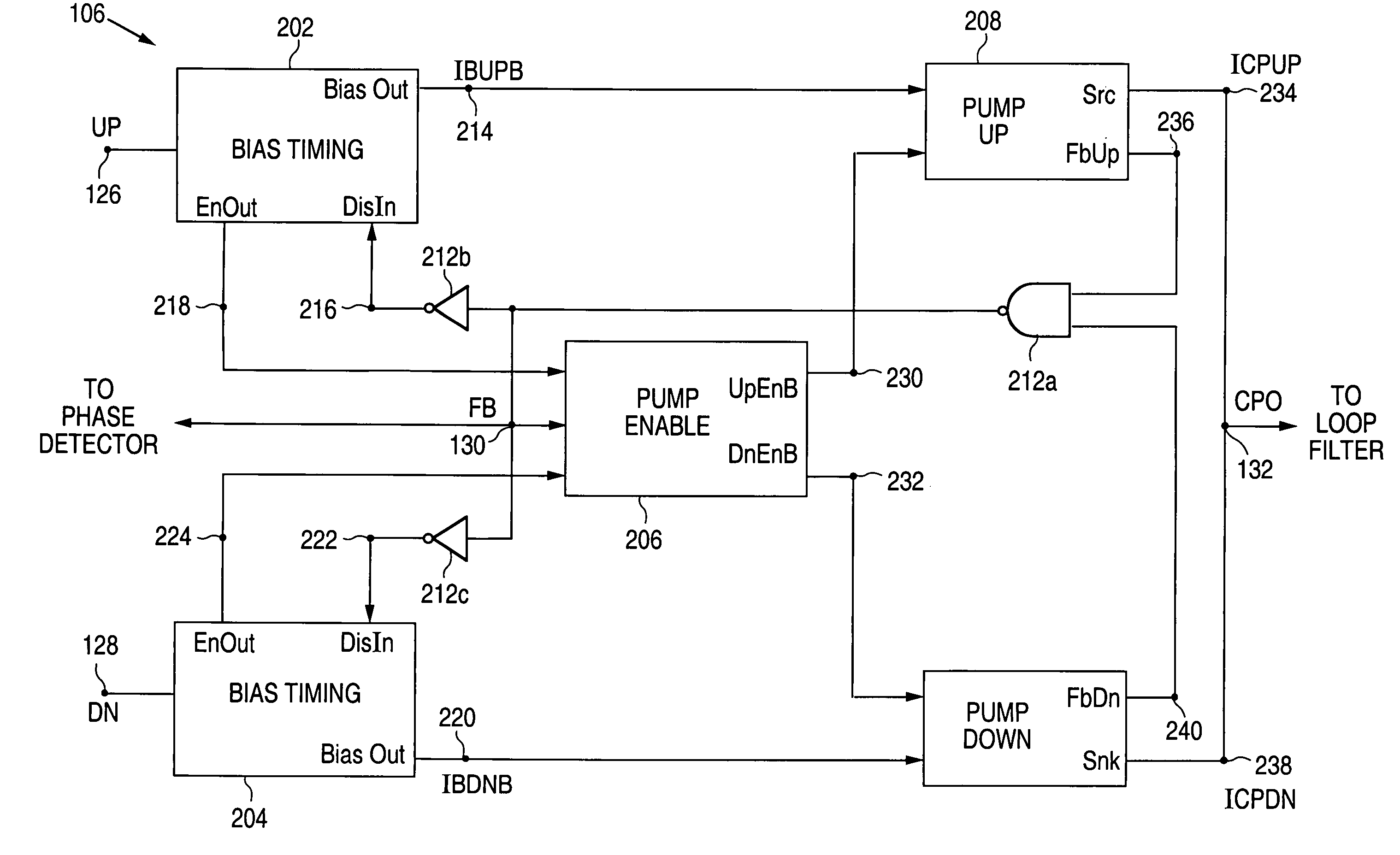
Figure 1 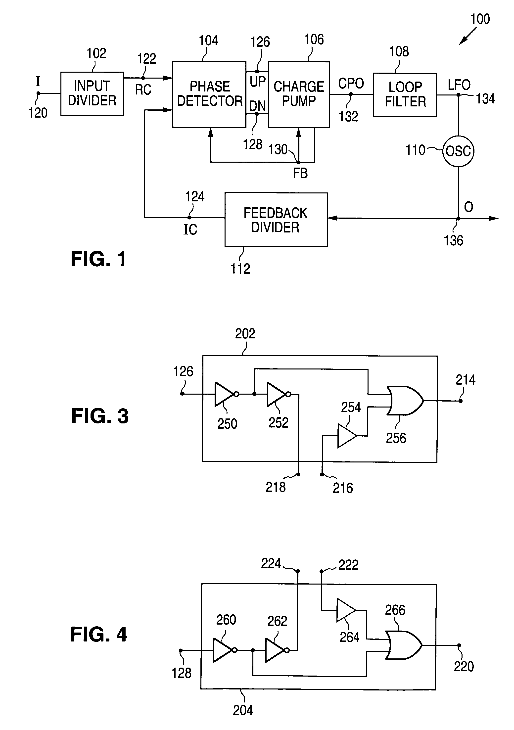
Figure 2 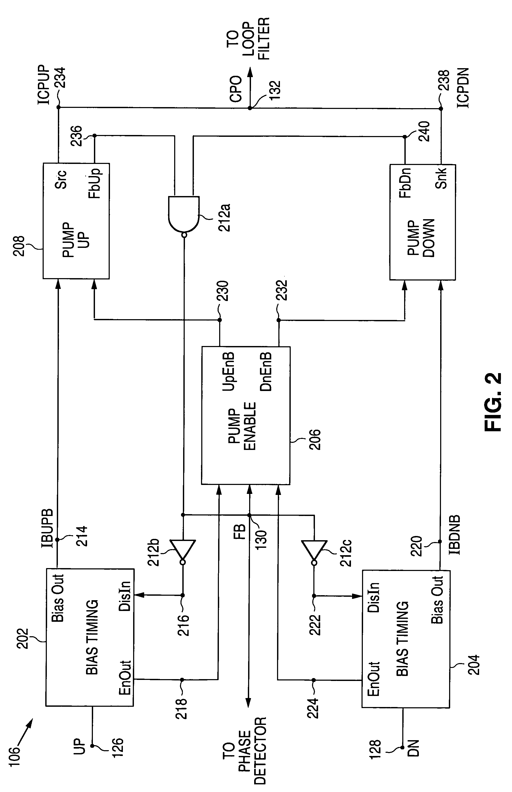
Figure 3
Abstract
Description
TECHNICAL FIELD OF THE INVENTION
[0001] The present invention relates generally to phase-locked loops and, more particularly, to a method and system for internally resetting a charge pump.BACKGROUND OF THE INVENTION
[0002] In many electronic systems, the clock signals that drive an integrated circuit are generated by a phase-locked loop (PLL) frequency synthesizer. The performance of the PLL frequency synthesizer is dependent on several parameters, including a minimum charge pump pulse width and corresponding phase noise. The minimum charge pump pulse width is limited by a feedback signal propagation time, which is the amount of time for a feedback signal from the charge pump to reset the phase detector and to propagate back through to the charge pump. The corresponding phase noise may not be reduced beyond the limits of the minimum charge pump pulse width.
[0003] In addition, some currently available PLL frequency synthesizers include one or more delay circuits to provide time-delayed ph...
Examples
Embodiment Construction
[0019]FIGS. 1 through 7, discussed below, and the various embodiments used to describe the principles of the present invention in this patent document are by way of illustration only and should not be construed in any way to limit the scope of the invention. Those skilled in the art will understand that the principles of the present invention may be implemented in any suitably arranged phase-locked loop frequency synthesizer.
[0020]FIG. 1 is a block diagram illustrating a phase-locked loop (PLL) frequency synthesizer 100 in accordance with one embodiment of the present invention. The PLL frequency synthesizer 100 is operable to provide an internal clock signal for an integrated circuit or other suitable device that is synchronous to an external clock signal.
[0021]The PLL frequency synthesizer 100 comprises an input divider 102, a phase detector 104, a charge pump 106, a loop filter 108, an oscillator 110, and a feedback divider 112. The input divider 102 is operable to receive an inp...