
Semiconductor package
a technology of semiconductors and packaging, applied in the direction of semiconductor devices, semiconductor/solid-state device details, electrical apparatus, etc., can solve the problems of low production yield, high production cost, and complicated transfer steps of insulating layers, etc., and achieve high production yield, high density packaging, and easy to use
Patent Information
- Authority / Receiving Office
- US · United States
- Patent Type
- Patents(United States)
- Current Assignee / Owner
- Publication Date
- 2008-05-27
- Estimated Expiration
- Not applicable · inactive patent
Smart Images
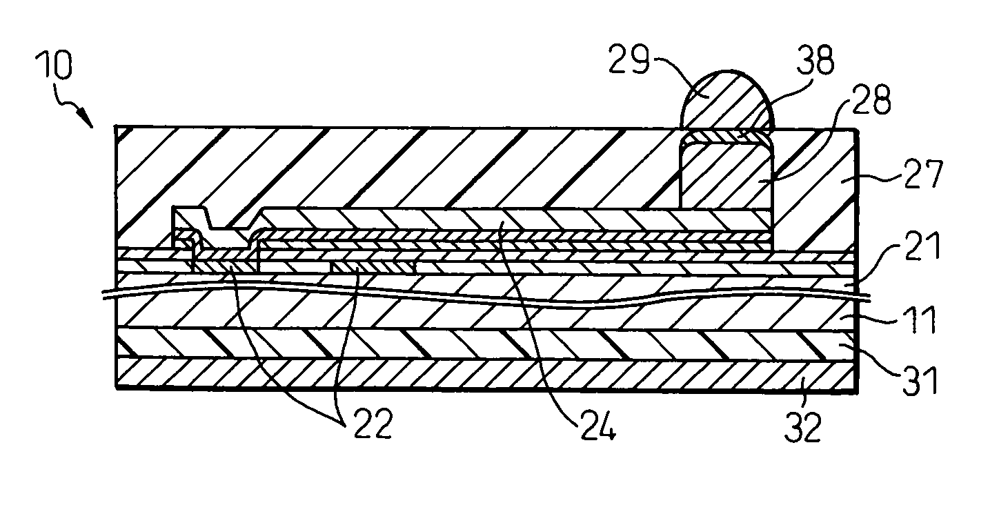
Figure 1 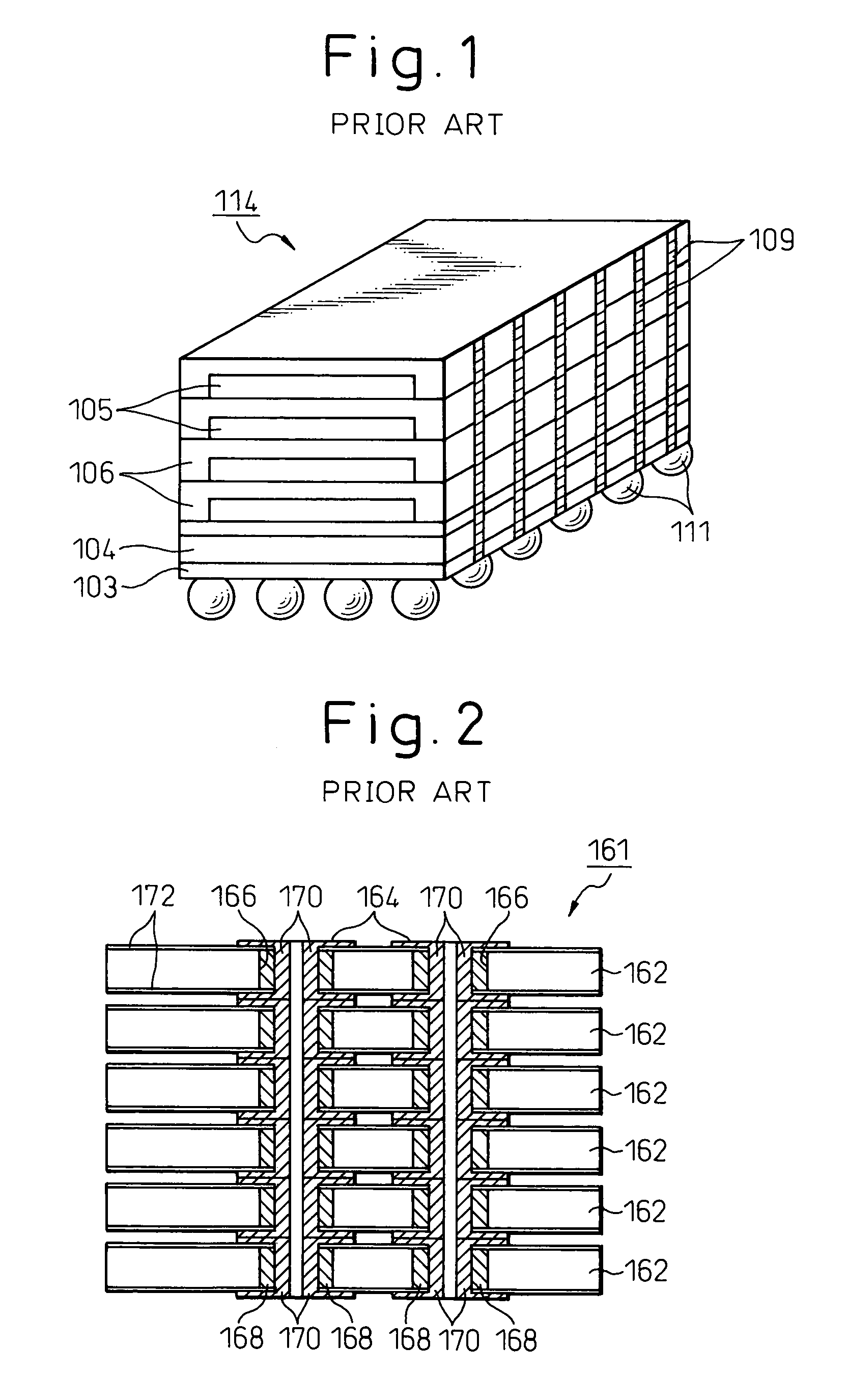
Figure 2 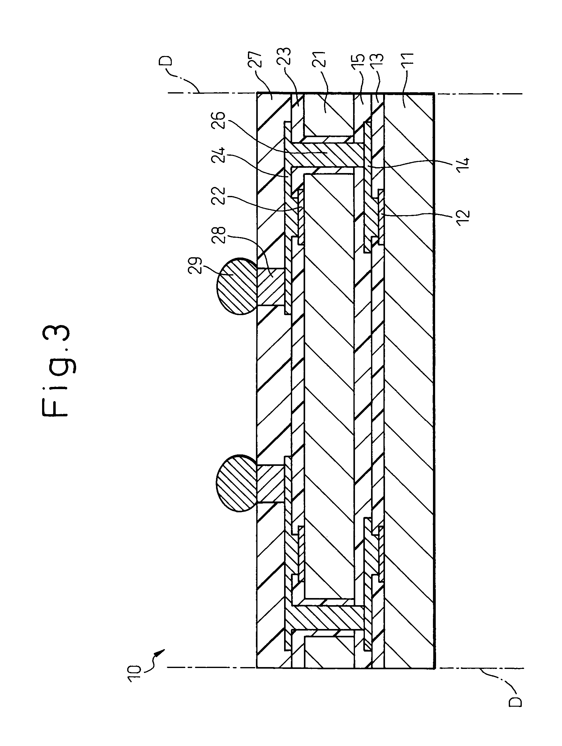
Figure 3
Abstract
Description
BACKGROUND OF THE INVENTION
[0001] 1. Field of the Invention
[0002] This invention relates to a semiconductor package having semiconductor devices packaged onto a substrate. More particularly, the invention relates to a small and high-performance semiconductor package capable of high-density packaging or a so-called “CSP (chip size package)”. The invention further relates to a method of producing such a semiconductor package easily, and at a high yield, at a wafer level.
[0003] 2. Description of Related Art
[0004] To cope with the higher performance and the reduction in size, so-called, “down sizing”, of electronic appliances, various types of semiconductor packages have been proposed, in recent years, which combine semiconductor devices such as IC chips, LSI chips, etc, or semiconductor devices having semiconductor chips mounted onto a substrate. To accomplish high-density packaging in such a semiconductor package, various research institutes and companies have proposed models of three-dim...
Examples
examples
[0044]Next, examples of the invention will be explained with reference to the accompanying drawings. Note, however, that the invention is not limited to the following examples. In the following explanation of the production method of the semiconductor package, one semiconductor package is shown in magnification for the purpose of simplification of the explanation. In practice, however, as the production is performed in the wafer level, the production method that collectively and batchwise fabricates a large number of semiconductor packages into one wafer and dices the wafer into discrete semiconductor packages, is used.
[0045]FIG. 3 is a sectional view showing a preferred example of the semiconductor package according to the invention. The semiconductor package 10 is produced by fabricating a large number of semiconductor devices into a silicon wafer in accordance with a predetermined design and dicing the wafer along a dicing line “D”. In the illustrated semiconductor package 10, a ...