
Staggered-pins structure for substrate
A staggered arrangement and pin structure technology, applied in electrical components, electrical solid devices, circuits, etc., can solve the problem of not being able to maximize the use of pin space, and achieve the effect of reducing size and high-density packaging.
Patent Information
- Authority / Receiving Office
- CN · China
- Current Assignee / Owner
- Publication Date
- 2012-07-25
Smart Images
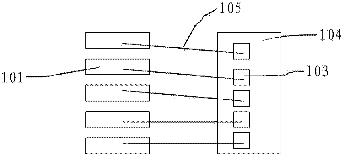
Figure 1 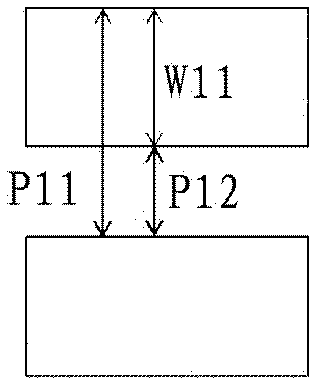
Figure 2 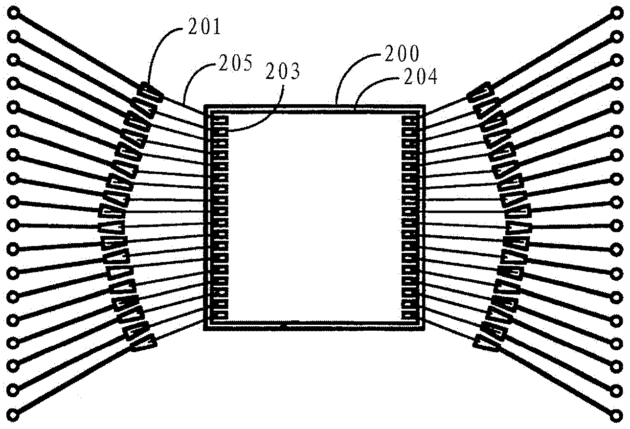
Figure 3
Abstract
Description
technical field
[0001] The invention belongs to the technical field of semiconductor packaging, in particular, the invention relates to a staggered pin structure for a substrate of a semiconductor package capable of realizing high-density integration. Background technique
[0002] As electronics become smaller, denser and perform better, semiconductors become proportionally smaller as their components and connections become denser. Generally, in order to realize circuit connection, bonding wires are used to connect substrate pins and chip ports through a wire bonding process. The wire bonding process is the use of bonding wires to connect the terminals of an integrated circuit (IC) chip (hereinafter referred to as "pads") to corresponding pins (sometimes referred to as "pads") such as a substrate or printed circuit board (PCB). wire bond pads” or “bond pads”) interconnections are known methods.
[0003] Conventional pads for wire bonding are regularly arranged, and the lea...
Examples
Embodiment Construction
[0027] Hereinafter, the present invention will be described more fully with reference to the accompanying drawings, in which exemplary embodiments of the invention are shown. As those skilled in the art would realize, the described embodiments may be modified in various different ways, all without departing from the spirit or scope of the principles employed in the invention.
[0028] It should be appreciated that the dimensions of the constituent members shown in the drawings are arbitrarily given for better understanding and ease of description, and the present invention is not limited by the illustrated dimensions. In the drawings, the thicknesses of layers, regions, etc., are exaggerated for clarity. The same or similar reference numerals denote the same elements throughout the specification.
[0029] The invention provides a new type of staggered regular hexagonal pins for the substrate, which is used to realize high-density wiring, and at the same time reduce the area o...