
Overvoltage-protected light-emitting semiconductor device, and method of fabrication
a technology of overvoltage protection and semiconductor devices, applied in semiconductor devices, semiconductor/solid-state device details, electrical apparatus, etc., can solve the problems of inability to meet the requirements of electrostatic breakdown, inability to resist electrostatic breakdown, and unsatisfactory solutions, etc., to achieve convenient and economical manufacture, improve the effect of reverse voltage, and reduce the size of the devi
Patent Information
- Authority / Receiving Office
- US · United States
- Patent Type
- Patents(United States)
- Current Assignee / Owner
- Publication Date
- 2011-03-01
- Estimated Expiration
- Not applicable · inactive patent
Smart Images
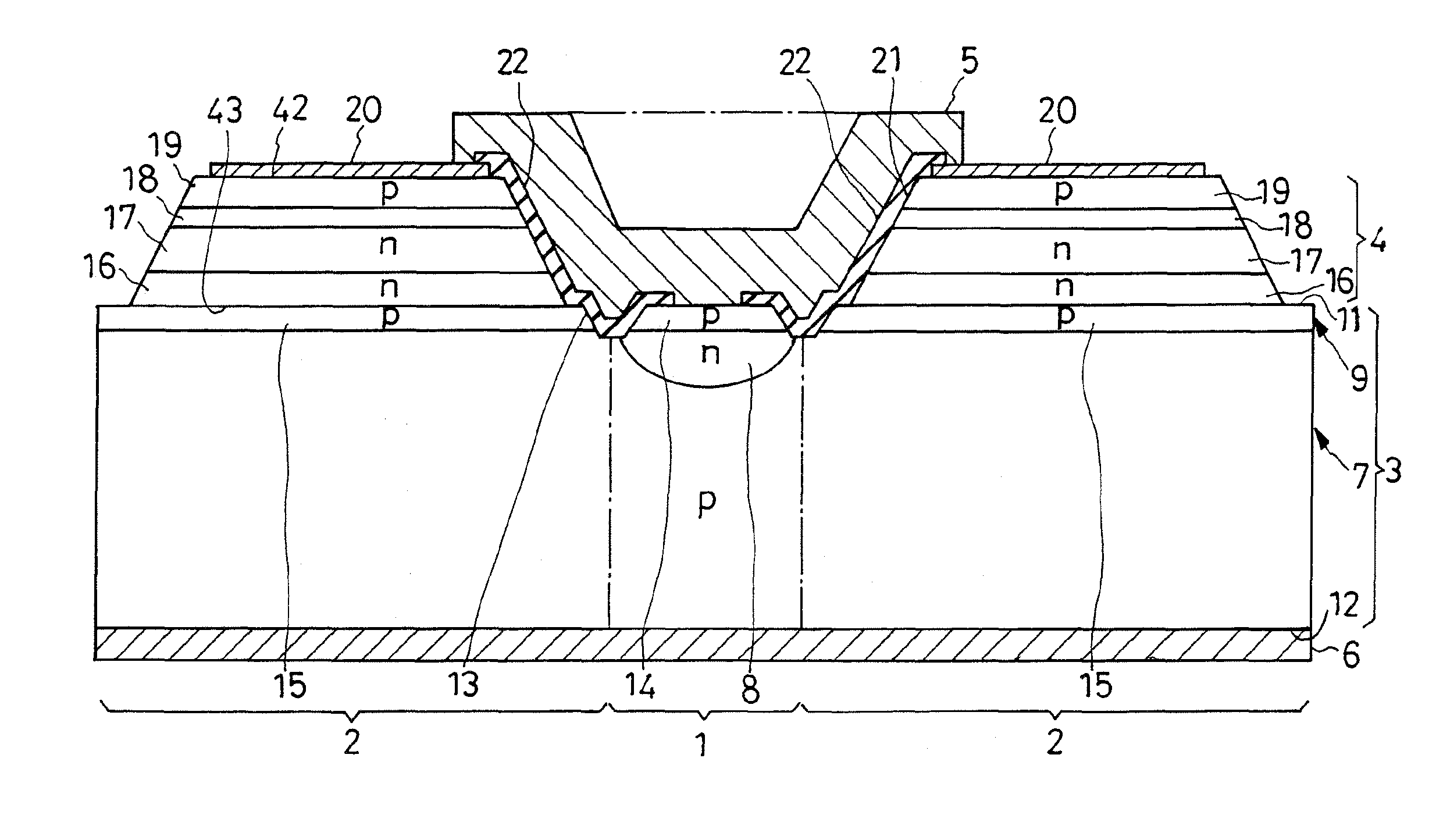
Figure 1 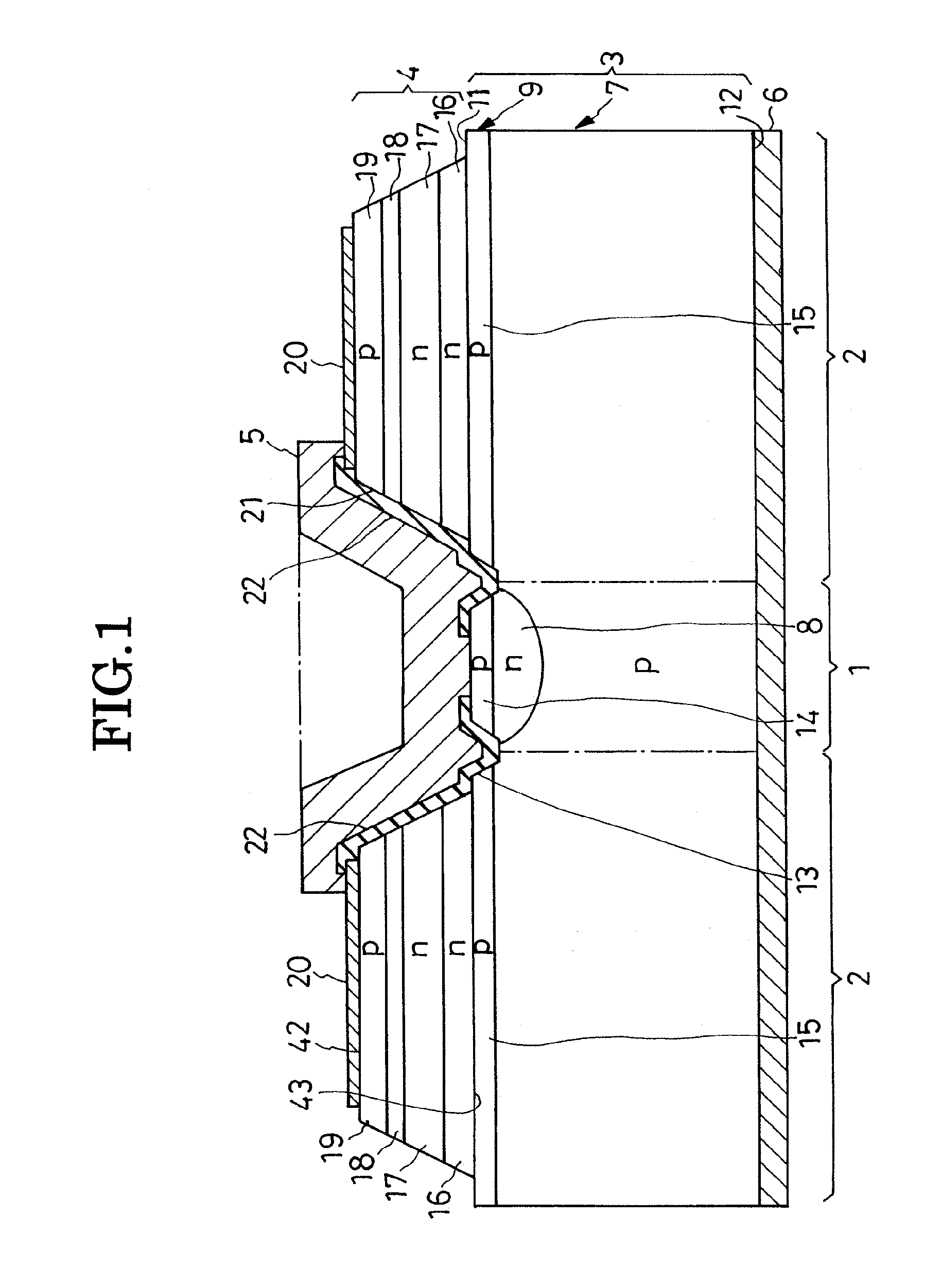
Figure 2 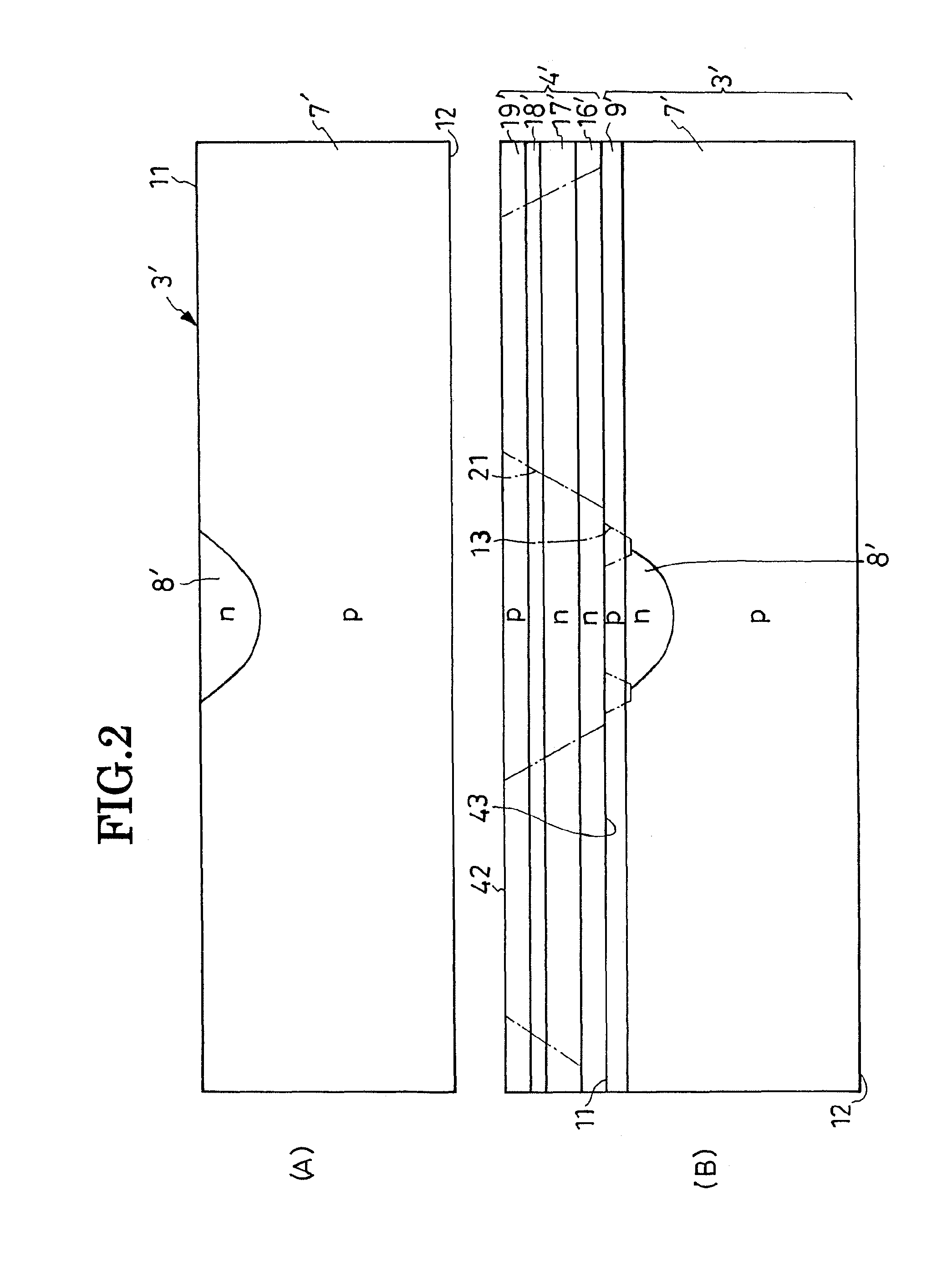
Figure 3
Abstract
Description
CROSS REFERENCE TO RELATED APPLICATIONS
[0001] This is a continuation of Application PCT / JP2007 / 050923, filed Jan. 22, 2007, which claims priority to Japanese Patent Application No. 2006-020242 filed Jan. 30, 2006.BACKGROUND OF THE INVENTION
[0002] This invention relates to a light-emitting semiconductor device, or light-emitting diode (LED) in common parlance, and more specifically to an LED featuring provisions for protection against overvoltages. The invention also specifically concerns a method of fabricating such an overvoltage-protected LED.
[0003] A host of specialists in electroluminescence have focused their attention in recent years on nitride semiconductors as LED materials. LEDs built from these materials emit light in the wavelength range of 365-550 nanometers. These devices have, however, an inherent weakness in withstanding electrostatic breakdown, being susceptible to destruction when subjected to a voltage surge in excess of 100 volts. It might be contemplated to incorpor...
Examples
Embodiment Construction
[0032]The present invention is believed to be best embodied in the overvoltage-protected LED illustrated in FIG. 1 of the above drawings. The representative LED includes a silicon substrate 3 which may be notionally divided into an overvoltage protector section 1 and LED section 2. The overvoltage protector section 1, at the central part of the substrate 3, is configured to provide overvoltage protector diodes according to the invention. The LED section 2 surrounds the overvoltage protector section 1 and supports a light-generating semiconductor region 4 thereon. Deposited on the LED section 2, the light-generating semiconductor region 4 is in the form of a lamination of several constituent layers for conventionally generating light. A front or top electrode 5 and back or bottom electrode 6 are disposed opposite each other across the substrate 3 and light-generating semiconductor region 4.
[0033]The substrate 3 is mostly constituted of a region 7 of p-type silicon and additionally ha...