
Fine pitch copper pillar package and method
a copper pillar and fine pitch technology, applied in the field of electronic components, can solve the problems of increasing the diameter of the solder bump, prone to failure, and delicate fine pitch solder bumps, and achieve the effect of maximizing the load bearing area of the copper pillar
Patent Information
- Authority / Receiving Office
- US · United States
- Patent Type
- Patents(United States)
- Current Assignee / Owner
- Publication Date
- 2013-09-17
Smart Images
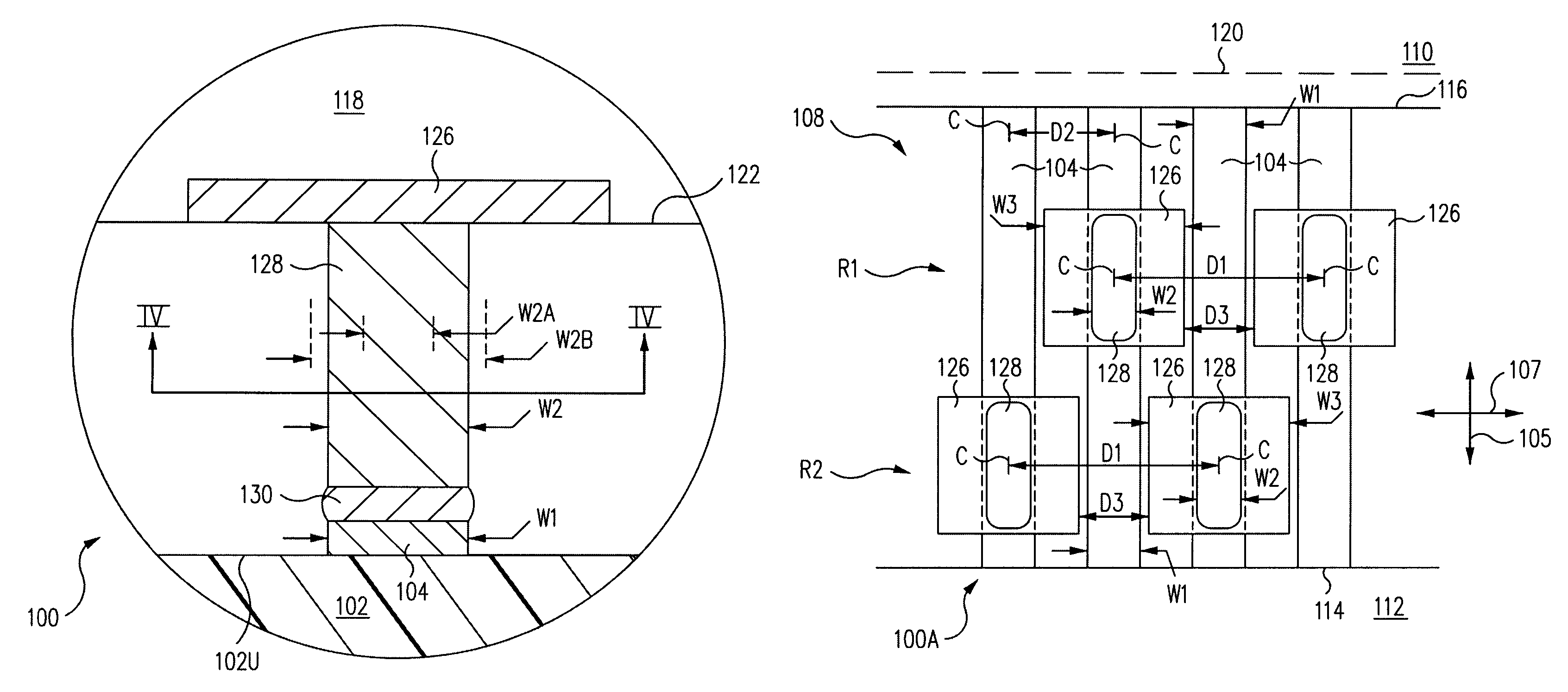
Figure 1 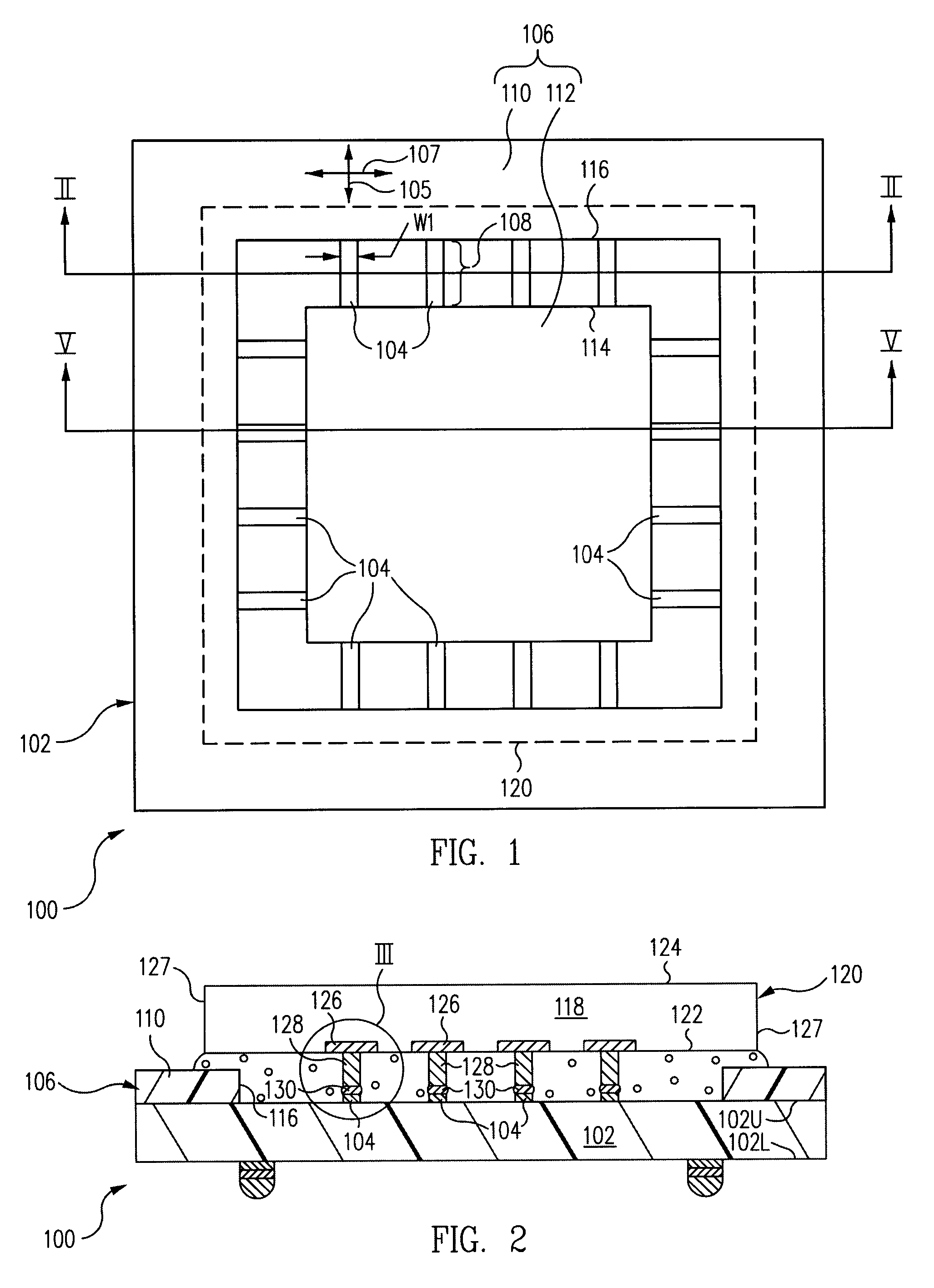
Figure 2 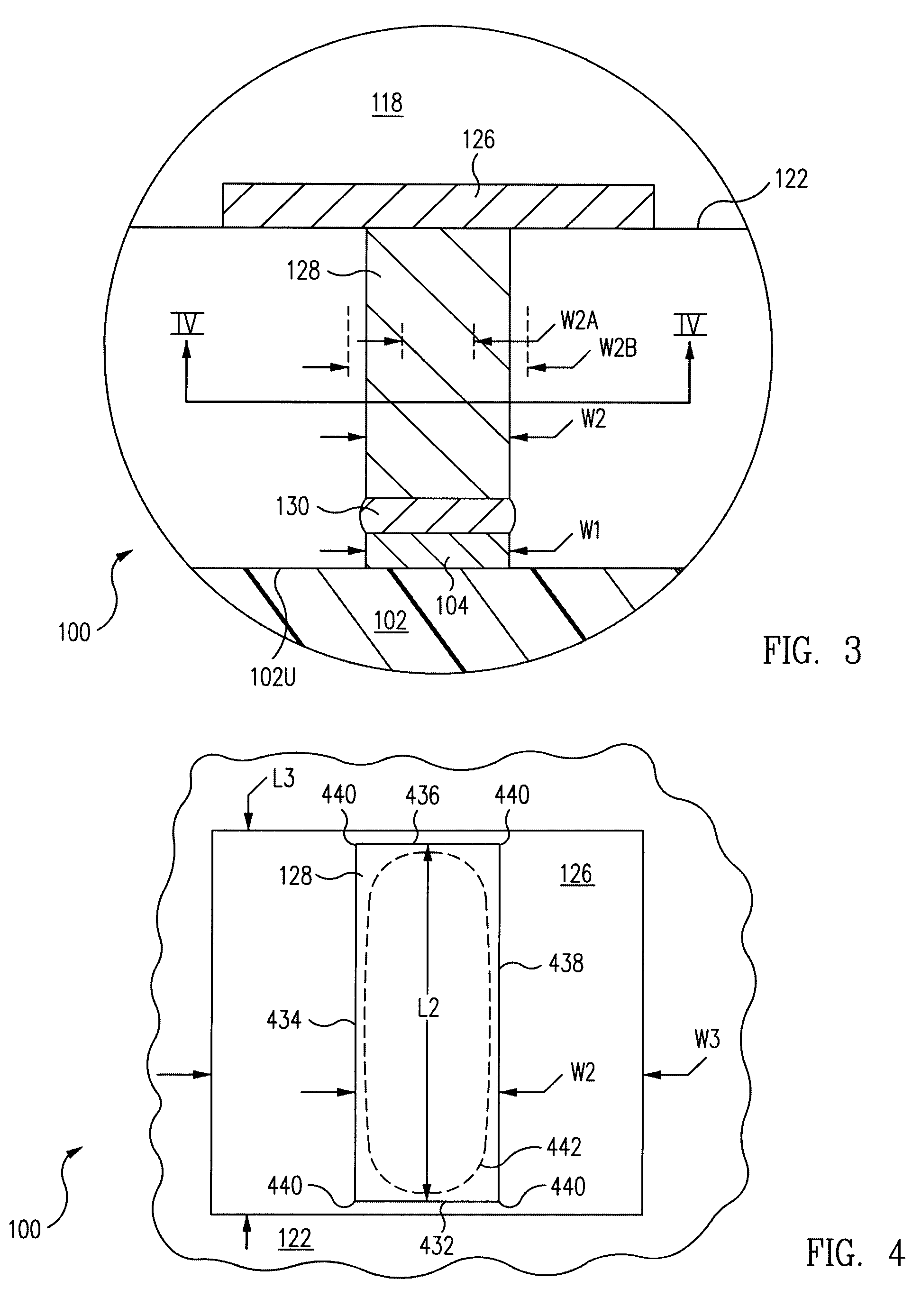
Figure 3
Abstract
Description
BACKGROUND OF THE INVENTION
[0001] 1. Field of the Invention
[0002] The present application relates to the field of electronics, and more particularly, to methods of forming electronic component packages and related structures.
[0003] 2. Description of the Related Art
[0004] Fine pitch flip chip technology requires very tight pad to pad spacing on the substrate and very tight bond pad to bond pad spacing on the integrated circuit chip. The pads of the substrate are electrically and physically connected to the bond pads of the integrated circuit chip using fine pitch solder bumps.
[0005] These fine pitch solder bumps are delicate and prone to failure due to the differential thermal expansion between the substrate and the integrated circuit chip. More particularly, the load bearing area of the solder bumps is very small and thus the stresses applied thereon are very high due to the thermal expansion mismatch between the integrated circuit chip and the substrate.
[0006] To increase the load bearin...
Examples
Embodiment Construction
[0023]FIG. 1 is top plan view of a fine pitch copper pillar package 100 in accordance with one embodiment. FIG. 2 is a cross-sectional view of fine pitch copper pillar package 100 along the line II-II of FIG. 1 in accordance with one embodiment.
[0024]Referring now to FIGS. 1 and 2 together, fine pitch copper pillar package 100, sometimes called an electronic component package, includes a substrate 102 including an upper, e.g., first, surface 102U and an opposite lower, e.g., second, surface 102L. Substrate 102 is a dielectric material such as laminate, ceramic, printed circuit board material, or other dielectric material.
[0025]Formed on upper surface 102U of substrate 102 are electrically conductive upper, e.g., first, traces 104. Also formed on upper surface 102U is a dielectric solder mask 106. Solder mask 106 has formed therein a window 108, sometimes called an opening or a trench in solder mask 106. Portions of upper traces 104 are exposed through window 108 thus facilitating el...