

Advanced Semiconductor Uses in Flexible OLED Encapsulation
SEP 28, 20259 MIN READ
Generate Your Research Report Instantly with AI Agent
PatSnap Eureka helps you evaluate technical feasibility & market potential.
Flexible OLED Encapsulation Technology Evolution and Objectives
Flexible OLED (Organic Light-Emitting Diode) technology has undergone significant evolution since its inception in the late 1990s. The journey began with rudimentary flexible displays that suffered from severe degradation due to oxygen and moisture penetration. Early encapsulation methods relied on rigid glass barriers that limited flexibility and application potential, creating a fundamental contradiction between protection and flexibility.
The mid-2000s marked a pivotal shift with the introduction of thin-film encapsulation (TFE) techniques, which represented the first viable approach to maintaining both barrier properties and flexibility. This period saw the emergence of multi-layer structures alternating organic and inorganic materials, establishing the foundation for modern encapsulation technologies.
By 2010-2015, atomic layer deposition (ALD) emerged as a breakthrough technology, enabling the creation of ultra-thin yet highly effective barrier films. This advancement significantly reduced water vapor transmission rates (WVTR) from 10^-3 g/m²/day to below 10^-6 g/m²/day, a critical threshold for commercial OLED viability.
The semiconductor industry's contribution became increasingly prominent post-2015, with advanced materials science driving innovation. Silicon-based compounds, metal oxides, and hybrid organic-inorganic materials developed for semiconductor manufacturing found new applications in OLED encapsulation. These materials offered unprecedented combinations of transparency, flexibility, and barrier properties.
Current technological objectives focus on several key areas: achieving WVTR below 10^-7 g/m²/day while maintaining mechanical flexibility for fold and roll capabilities; developing encapsulation layers less than 10μm thick that can withstand over 200,000 folding cycles; and creating manufacturing processes compatible with high-volume production at reduced costs.
The integration of semiconductor-grade materials represents a particularly promising direction, with aluminum oxide, silicon nitride, and hybrid organic-inorganic composites showing exceptional barrier properties. Advanced deposition techniques borrowed from semiconductor fabrication, including plasma-enhanced ALD and spatial ALD, are enabling precise control over film morphology and defect density.
Looking forward, the technology roadmap aims to develop "self-healing" encapsulation layers that can automatically repair microcracks formed during mechanical stress. Additionally, there is growing interest in environmentally sustainable encapsulation materials that maintain performance while reducing environmental impact throughout the product lifecycle.
The convergence of semiconductor and display technologies continues to drive innovation, with research institutions and industry leaders collaborating to overcome the fundamental challenges of protecting sensitive OLED materials while enabling the flexibility that next-generation displays demand.
Market Analysis for Advanced Semiconductor-Based OLED Encapsulation
The global market for advanced semiconductor-based OLED encapsulation technologies is experiencing robust growth, driven primarily by the expanding flexible display industry. Current market valuations indicate that the OLED encapsulation segment reached approximately 1.8 billion USD in 2022, with projections suggesting a compound annual growth rate (CAGR) of 15.7% through 2028. This growth trajectory is significantly outpacing traditional display technologies, reflecting the increasing consumer preference for flexible, durable display solutions.
Consumer electronics remains the dominant application sector, accounting for over 65% of the market share. Within this segment, smartphones and wearable devices are the primary drivers, with premium smartphone manufacturers increasingly adopting flexible OLED displays as a standard feature in flagship models. The wearable technology market, particularly smartwatches and fitness trackers, represents the fastest-growing subsegment with a CAGR exceeding 20%.
Regional analysis reveals that East Asia continues to dominate the production landscape, with South Korea, Japan, and Taiwan collectively controlling approximately 78% of the advanced encapsulation technology market. However, China is rapidly expanding its market presence through substantial investments in domestic OLED manufacturing capabilities, with its market share growing from 8% in 2018 to nearly 18% in 2022.
Demand-side factors indicate strong consumer willingness to pay premium prices for devices featuring flexible displays, with market surveys showing that 72% of high-end smartphone purchasers consider foldable or flexible display options as "highly desirable." This consumer sentiment is reinforced by the growing ecosystem of applications optimized for flexible display formats.
Supply chain analysis reveals increasing vertical integration among major players, with semiconductor manufacturers expanding into specialized encapsulation materials and processes. This trend is partially driven by efforts to mitigate supply chain vulnerabilities exposed during recent global disruptions. Material costs remain a significant factor, with advanced barrier films and semiconductor-based encapsulation layers contributing approximately 22% to the overall manufacturing cost of flexible OLED panels.
Market forecasts suggest that emerging applications in automotive displays, augmented reality devices, and smart home interfaces will create new growth vectors for advanced encapsulation technologies. The automotive sector, in particular, is projected to increase its market share from 5% to 12% by 2026, driven by the integration of curved and flexible displays in vehicle interiors.
Current Semiconductor Technologies and Barriers in OLED Encapsulation
Current semiconductor technologies for flexible OLED encapsulation primarily focus on thin-film barrier solutions that protect sensitive organic materials from moisture and oxygen degradation. Atomic Layer Deposition (ALD) represents the most advanced approach, enabling the creation of ultra-thin aluminum oxide (Al2O3) and silicon nitride (Si3N4) layers with thickness precision at the atomic level. These films provide exceptional barrier properties while maintaining the flexibility required for next-generation display applications.
Multi-layer barrier structures, alternating inorganic and organic layers, have emerged as the industry standard. The inorganic layers (typically metal oxides) serve as the primary moisture barrier, while organic interlayers accommodate mechanical stress during bending. This architecture, known as Thin-Film Encapsulation (TFE), has largely replaced traditional glass encapsulation in flexible displays.
Plasma-Enhanced Chemical Vapor Deposition (PECVD) remains widely utilized for depositing silicon oxide and silicon nitride layers, offering good throughput and cost-effectiveness. However, PECVD films typically contain more defects than ALD alternatives, necessitating thicker layers or multiple deposition cycles to achieve comparable barrier performance.
Despite significant advancements, several critical barriers persist in current semiconductor-based encapsulation technologies. The most pressing challenge involves the "pinhole problem" - microscopic defects in thin films that create pathways for moisture penetration. Even nanoscale defects can lead to progressive OLED degradation, manifesting as dark spots that expand over time.
Mechanical durability presents another substantial hurdle. Inorganic barrier films, while excellent at blocking moisture, tend to crack under repeated bending stress. This limitation constrains the minimum bend radius achievable in flexible displays and reduces overall device lifespan through cyclic mechanical fatigue.
Process integration challenges also remain significant. The temperature sensitivity of OLED materials (typically degrading above 100°C) restricts the processing window for encapsulation deposition. This limitation forces compromises between optimal barrier properties and maintaining OLED integrity during manufacturing.
Cost and scalability concerns further complicate widespread adoption. ALD processes, while producing superior films, suffer from relatively slow deposition rates compared to alternatives like sputtering or PECVD. This throughput limitation increases production costs and creates bottlenecks in high-volume manufacturing environments.
Edge sealing represents another persistent technical challenge. While the active display area may be well-protected by thin-film barriers, moisture ingress often occurs at the edges where different materials interface. Advanced edge sealing technologies using hybrid organic-inorganic materials are under development but have yet to achieve ideal performance in production environments.
Semiconductor Solutions for Flexible OLED Encapsulation
01 Encapsulation materials for semiconductor devices
Various materials are used for encapsulating semiconductor devices to protect them from environmental factors and enhance their reliability. These materials include polymers, resins, and composite materials that provide mechanical protection, thermal management, and electrical insulation. The encapsulation materials are selected based on their properties such as thermal conductivity, coefficient of thermal expansion, and moisture resistance to ensure optimal performance of the semiconductor devices.- Encapsulation materials for semiconductor devices: Various materials are used for encapsulating semiconductor devices to protect them from environmental factors and enhance their reliability. These materials include polymers, resins, and composite materials that provide mechanical protection, thermal management, and electrical insulation. The encapsulation materials are selected based on their properties such as thermal conductivity, coefficient of thermal expansion, and moisture resistance to ensure optimal performance of the semiconductor devices.
- Encapsulation techniques for LED and optoelectronic devices: Specialized encapsulation methods are developed for light-emitting diodes (LEDs) and other optoelectronic devices. These techniques focus on maintaining optical transparency while providing protection from environmental factors. The encapsulation processes may involve the use of silicone materials, epoxy resins, or other transparent polymers that can withstand high temperatures and provide optimal light extraction efficiency. Advanced techniques may also incorporate phosphors or other materials to modify the optical properties of the emitted light.
- Wafer-level encapsulation processes: Wafer-level encapsulation (WLE) involves encapsulating semiconductor devices at the wafer level before they are singulated into individual chips. This approach offers advantages in terms of manufacturing efficiency, miniaturization, and cost reduction. WLE techniques include the deposition of thin film layers, application of molding compounds, or bonding of cap wafers. These processes provide hermetic or near-hermetic sealing to protect sensitive components from moisture, contaminants, and mechanical stress.
- Encapsulation for battery and energy storage semiconductor technologies: Encapsulation solutions specifically designed for semiconductor-based energy storage devices, including batteries and supercapacitors. These encapsulation methods focus on preventing electrolyte leakage, managing thermal issues, and ensuring long-term stability of the energy storage components. The encapsulation materials must be resistant to the chemical environment of the battery while maintaining flexibility to accommodate volume changes during charge-discharge cycles. Advanced techniques may incorporate barrier layers to prevent moisture ingress and improve the overall lifetime of the energy storage devices.
- Advanced packaging and 3D integration encapsulation: Encapsulation technologies for advanced semiconductor packaging and three-dimensional (3D) integration. These methods address the challenges of interconnecting and protecting stacked die arrangements, through-silicon vias (TSVs), and heterogeneous integration platforms. The encapsulation processes may involve the use of underfill materials, molding compounds, or adhesives that provide mechanical support, thermal management, and electrical isolation between the integrated components. These techniques enable higher integration density, improved performance, and enhanced reliability for complex semiconductor systems.
02 Encapsulation techniques for LED and optoelectronic devices
Specialized encapsulation methods are employed for light-emitting diodes (LEDs) and other optoelectronic devices to enhance light extraction efficiency and protect the sensitive components. These techniques include using transparent or translucent encapsulants, incorporating phosphors for color conversion, and designing specific encapsulation geometries to optimize optical performance. The encapsulation process also addresses thermal management challenges unique to optoelectronic devices.Expand Specific Solutions03 Advanced packaging technologies for semiconductor integration
Advanced packaging technologies enable higher levels of semiconductor integration through innovative encapsulation approaches. These include wafer-level packaging, system-in-package (SiP), and 3D integration techniques that allow for multiple semiconductor components to be encapsulated together. Such approaches minimize form factors, improve electrical performance by reducing interconnect lengths, and enhance thermal management through optimized encapsulation designs.Expand Specific Solutions04 Encapsulation methods for power semiconductor devices
Power semiconductor devices require specialized encapsulation methods to handle high voltage, current, and temperature conditions. These methods focus on enhancing thermal dissipation, providing electrical isolation, and ensuring long-term reliability under harsh operating conditions. Techniques include using high thermal conductivity materials, incorporating heat spreaders within the encapsulation, and designing specific structures to manage thermal stress and electrical field distribution.Expand Specific Solutions05 Environmental protection and reliability enhancement in semiconductor encapsulation
Encapsulation technologies are developed to enhance the environmental protection and reliability of semiconductor devices. These include moisture-resistant encapsulants, hermetic sealing techniques, and materials that provide protection against mechanical shock, vibration, and temperature cycling. Advanced approaches incorporate stress-relieving designs and materials with matched coefficients of thermal expansion to minimize failures due to environmental factors and extend device lifetime.Expand Specific Solutions
Key Industry Players in Semiconductor-Based OLED Encapsulation
The flexible OLED encapsulation market is currently in a growth phase, with an estimated market size exceeding $2 billion and projected to expand significantly as demand for flexible displays increases. Technologically, the field is advancing from early-stage development to commercial maturity, with varying levels of expertise among key players. Asian manufacturers dominate the competitive landscape, with BOE Technology, LG Display, and Tianma Microelectronics leading in production capacity and technological innovation. Chinese companies like Visionox and TCL CSOT are rapidly advancing their capabilities, while Applied Materials provides critical manufacturing equipment. The technology is approaching maturity for standard applications, but advanced solutions for ultra-thin and highly flexible displays remain challenging, with companies focusing on barrier film technologies and atomic layer deposition methods to improve encapsulation performance.
BOE Technology Group Co., Ltd.
Technical Solution: BOE has developed a comprehensive semiconductor-based encapsulation solution for flexible OLED displays centered around their "Multi-Buffer Layer" technology. This approach utilizes alternating layers of inorganic silicon nitride (SiNx) and silicon oxynitride (SiOxNy) films deposited through plasma-enhanced atomic layer deposition (PEALD) at temperatures below 100°C. The inorganic layers provide excellent barrier properties while the organic buffer layers absorb mechanical stress during bending. BOE's proprietary process achieves ultra-thin barrier films with thicknesses of 3-5nm per layer while maintaining high uniformity across large substrates. Their latest innovation incorporates quantum dot-enhanced barrier films that not only provide encapsulation but also enhance color performance. BOE has also pioneered the integration of thin-film transistor (TFT) backplanes with their encapsulation technology, allowing for seamless production of flexible displays with reduced manufacturing steps.
Strengths: Highly scalable process suitable for Gen 8.5+ substrates; excellent barrier properties with WVTR below 10^-6 g/m²/day; integrated approach combining encapsulation with other display components. Weaknesses: Higher initial capital investment for specialized deposition equipment; challenges with uniformity control across very large substrates; relatively new to mass production compared to some competitors.
LG Display Co., Ltd.
Technical Solution: LG Display has pioneered advanced thin-film encapsulation (TFE) technology for flexible OLED displays, utilizing a multi-layer structure that alternates inorganic and organic materials. Their proprietary technology employs atomic layer deposition (ALD) to create ultra-thin barrier films of Al2O3 and SiO2 with thicknesses below 10nm, combined with organic polymer layers. This sandwich structure effectively prevents moisture and oxygen penetration while maintaining flexibility. LG has further enhanced this technology with their "Hybrid Passivation Layer" approach, incorporating silicon nitride layers deposited via plasma-enhanced chemical vapor deposition (PECVD) to achieve a water vapor transmission rate (WVTR) below 10^-6 g/m²/day. Their latest innovation includes integrating nanoparticle-enhanced barrier films that improve mechanical durability while reducing overall encapsulation thickness to under 10μm.
Strengths: Industry-leading barrier performance with extremely low WVTR; excellent mechanical flexibility allowing for repeated bending without degradation; mature mass production capability. Weaknesses: Higher production costs compared to conventional encapsulation; complex multi-step deposition process requiring precise control; potential yield issues at high-volume manufacturing.
Critical Patents and Innovations in Advanced Encapsulation Materials
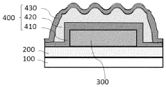
Flexible organic light-emitting diode (OLED) device of reduced stess at bending place and fabrication method thereof
PatentActiveUS11258038B2
Innovation
- A novel encapsulation layer configuration with a first and second inorganic layer and an organic layer, where the second inorganic layer has a continuous wavy curved configuration, formed by thermal stress differences, increasing contact area and reducing stress on the outer inorganic layer, and an optically clear adhesive is used to level the configuration.
Organic light-emitting diode encapsulation structure, method for fabricating the same, and organic light-emitting diode
PatentInactiveUS20190051857A1
Innovation
- An organic light-emitting diode encapsulation structure is developed, featuring a cover plate and array substrate bonded with frame sealing glue on a spacing layer with a concave-convex pattern, enhancing the bonding between the glue and the substrate, and optionally using an oxynitride or metal film layer to improve sealing without increasing the glue width.


Environmental Impact and Sustainability Considerations
The environmental footprint of flexible OLED encapsulation technologies represents a critical consideration as these displays gain market prominence. Traditional encapsulation methods often rely on materials with significant environmental concerns, including rare earth elements and compounds with high global warming potential. Advanced semiconductor approaches to OLED encapsulation offer promising alternatives that can substantially reduce these impacts through material efficiency and longevity improvements.
Thin-film encapsulation (TFE) technologies utilizing atomic layer deposition (ALD) demonstrate superior environmental performance compared to conventional methods. These processes require significantly less material input while achieving better barrier properties, resulting in up to 40% reduction in raw material consumption. Additionally, the precision of ALD processes minimizes waste generation during manufacturing, addressing a key sustainability challenge in semiconductor production.
Energy consumption during manufacturing remains a significant concern for advanced encapsulation technologies. Current ALD and plasma-enhanced chemical vapor deposition (PECVD) processes used in semiconductor-based encapsulation require substantial energy inputs, though recent innovations have reduced per-unit energy requirements by approximately 25% compared to earlier generations. Further efficiency improvements are being pursued through low-temperature deposition techniques and optimized process scheduling.
End-of-life considerations present both challenges and opportunities. The multi-layer nature of advanced semiconductor encapsulation systems complicates recycling efforts, as separation of nanometer-scale layers remains technically challenging. However, the extended lifetime of devices using these advanced encapsulation methods—often 30-50% longer than conventional alternatives—partially offsets this concern by reducing overall electronic waste generation rates.
Water usage in semiconductor-based encapsulation processes represents another environmental consideration. Current manufacturing approaches require ultra-pure water in substantial quantities, with estimates suggesting 5-7 liters per square meter of display area. Closed-loop water recycling systems are being implemented by leading manufacturers, achieving water reuse rates of up to 80% in advanced facilities.
Carbon footprint analyses indicate that while production-phase emissions for advanced semiconductor encapsulation are higher than conventional methods, the extended device lifetimes and reduced material requirements result in net lifecycle carbon reductions of approximately 15-20%. This calculation factors in both manufacturing emissions and avoided replacement production.
Regulatory frameworks worldwide are increasingly addressing the environmental aspects of display technologies. The European Union's Restriction of Hazardous Substances (RoHS) and Registration, Evaluation, Authorization and Restriction of Chemicals (REACH) regulations have particular implications for encapsulation materials selection, driving innovation toward more environmentally benign alternatives in semiconductor-based approaches.
Manufacturing Scalability and Cost Analysis
The scalability of manufacturing processes for flexible OLED encapsulation using advanced semiconductor technologies presents significant challenges and opportunities for industry stakeholders. Current production methods for thin-film encapsulation (TFE) layers involve complex deposition processes that require precise control of environmental conditions, including temperature, pressure, and contamination levels. These stringent requirements often result in lower throughput and higher production costs compared to traditional display manufacturing techniques.
Analysis of production economics reveals that material costs constitute approximately 40-45% of total manufacturing expenses for flexible OLED encapsulation, with advanced semiconductor materials like silicon nitride and aluminum oxide representing significant portions of this expenditure. Equipment depreciation accounts for another 30-35%, while labor and overhead costs make up the remainder. The capital expenditure required for establishing a production line capable of manufacturing advanced encapsulation solutions exceeds $100 million, creating substantial barriers to entry for new market participants.
Yield rates remain a critical challenge in scaling production, with current industry averages ranging from 70-85% for high-quality flexible encapsulation layers. Defect density in barrier films directly impacts device lifetime and performance, making quality control systems essential but adding further to production costs. The implementation of advanced process control systems utilizing machine learning algorithms has shown promise in improving yield rates by 10-15% in pilot production environments.
Recent innovations in atomic layer deposition (ALD) and plasma-enhanced chemical vapor deposition (PECVD) technologies have demonstrated potential for increasing throughput while maintaining film quality. Roll-to-roll processing techniques, adapted from semiconductor manufacturing, offer pathways to significant cost reductions, potentially decreasing production expenses by 25-30% when fully optimized. However, these approaches require substantial refinement before widespread industrial adoption.
Supply chain considerations also impact manufacturing scalability, with certain critical materials facing potential shortages as demand increases. Diversification of material sources and development of alternative encapsulation materials represent important strategies for mitigating supply risks. Additionally, regional manufacturing clusters have emerged in East Asia, particularly in South Korea, Japan, and Taiwan, where existing semiconductor infrastructure provides synergistic benefits for flexible OLED encapsulation production.
Future cost reduction trajectories suggest that economies of scale, process optimization, and material innovations could drive a 40-50% decrease in production costs over the next five years, potentially accelerating market adoption of flexible OLED technologies across consumer electronics, automotive, and emerging wearable device segments.
Unlock deeper insights with PatSnap Eureka Quick Research — get a full tech report to explore trends and direct your research. Try now!
Generate Your Research Report Instantly with AI Agent
Supercharge your innovation with PatSnap Eureka AI Agent Platform!