

Exploring Flexible OLED Encapsulation for Enhanced Optical Clarity
SEP 28, 20259 MIN READ
Generate Your Research Report Instantly with AI Agent
PatSnap Eureka helps you evaluate technical feasibility & market potential.
Flexible OLED Encapsulation Evolution and Objectives
Flexible OLED (Organic Light-Emitting Diode) technology has revolutionized display systems over the past decade, evolving from rigid structures to malleable interfaces that can bend, fold, and conform to various surfaces. The journey began in the early 2000s with the first demonstrations of flexible OLED prototypes, which suffered from severe degradation due to oxygen and moisture penetration. These early iterations exhibited limited flexibility, poor durability, and compromised optical performance.
By 2010, the industry had recognized encapsulation as the critical bottleneck in flexible OLED development. Traditional glass-based encapsulation methods, while effective for rigid displays, proved incompatible with the mechanical requirements of flexible applications. This realization sparked intensive research into alternative encapsulation technologies, particularly thin-film encapsulation (TFE) and hybrid approaches combining organic and inorganic layers.
The period between 2012 and 2016 marked significant breakthroughs in atomic layer deposition (ALD) techniques, enabling the creation of ultra-thin barrier films with exceptional moisture resistance. These advancements allowed for the first commercially viable flexible OLED products, though optical clarity remained compromised by the multiple barrier layers required for adequate protection.
From 2017 onward, the focus shifted toward enhancing optical performance while maintaining or improving barrier properties. The industry witnessed the emergence of nanocomposite materials and advanced hybrid encapsulation systems designed specifically to minimize light scattering and absorption while providing robust environmental protection.
Current technological objectives center on achieving the seemingly contradictory goals of superior optical clarity and enhanced barrier performance in increasingly flexible form factors. Researchers aim to develop encapsulation solutions that maintain transparency above 95% across the visible spectrum while achieving water vapor transmission rates below 10^-6 g/m²/day and enabling bend radii under 1mm without degradation.
Additional objectives include reducing encapsulation thickness to below 10 micrometers to enhance flexibility, developing manufacturing processes compatible with roll-to-roll production for cost reduction, and creating environmentally sustainable encapsulation materials that reduce reliance on rare earth elements and fluorinated compounds.
The ultimate goal is to enable a new generation of flexible OLED displays with perfect optical clarity, imperceptible encapsulation layers, and durability measured in years rather than months. This would unlock applications in foldable smartphones, rollable televisions, wearable displays, and conformable lighting solutions that seamlessly integrate into various environments and products.
Market Demand Analysis for High-Clarity Flexible Displays
The flexible display market has witnessed exponential growth in recent years, driven primarily by increasing consumer demand for portable, lightweight, and durable electronic devices. Market research indicates that the global flexible display market is projected to reach $42 billion by 2027, with a compound annual growth rate of 28% from 2022 to 2027. This remarkable growth trajectory underscores the significant market potential for high-clarity flexible displays across various industries.
Consumer electronics represents the largest application segment for flexible OLED displays, with smartphones accounting for approximately 65% of the total market share. Major smartphone manufacturers have increasingly adopted flexible displays in their flagship models, highlighting the premium nature and consumer appeal of this technology. The wearable technology sector follows closely, with smartwatches and fitness trackers incorporating flexible displays to enhance user experience and device functionality.
Market surveys reveal that consumers prioritize display quality as a critical factor in purchasing decisions, with 78% of respondents indicating that screen clarity significantly influences their choice of electronic devices. This consumer preference has intensified competition among manufacturers to develop displays with superior optical properties, including enhanced clarity, color accuracy, and brightness.
The automotive industry has emerged as a rapidly growing market for flexible displays, with an estimated market value of $3.5 billion by 2025. Luxury vehicle manufacturers are integrating curved and flexible displays into dashboards and entertainment systems, creating opportunities for high-clarity display technologies that can withstand automotive environmental conditions.
Regional analysis shows that Asia-Pacific dominates the flexible display market, accounting for 62% of global production capacity. This regional concentration is attributed to the presence of major display manufacturers and electronics companies in countries like South Korea, Japan, and China. North America and Europe follow as significant markets, driven by high consumer spending power and rapid technology adoption.
Industry forecasts indicate that demand for flexible displays with enhanced optical clarity will continue to grow as applications expand beyond traditional consumer electronics into emerging sectors such as healthcare, retail, and smart home devices. The healthcare segment, in particular, is expected to grow at 32% annually through 2026, with applications in medical monitoring devices and portable diagnostic equipment requiring high-clarity displays.
Market challenges include price sensitivity, as high-clarity flexible displays currently command a premium of 30-40% over conventional displays. However, as manufacturing processes mature and economies of scale are achieved, this price differential is expected to narrow, further accelerating market adoption across diverse product categories and price segments.
Current Encapsulation Technologies and Barriers
The flexible OLED encapsulation landscape is currently dominated by several key technologies, each with distinct advantages and limitations. Thin-film encapsulation (TFE) represents the most widely adopted solution, typically employing alternating layers of inorganic and organic materials. The inorganic layers (commonly silicon nitride or aluminum oxide) provide excellent barrier properties against moisture and oxygen, while the organic layers (often based on acrylate polymers) offer flexibility and stress relief. This multi-layer approach has demonstrated water vapor transmission rates (WVTR) below 10^-6 g/m²/day, meeting the stringent requirements for OLED protection.
Atomic Layer Deposition (ALD) has emerged as a critical process for creating high-quality barrier films with precise thickness control at the atomic level. ALD-deposited Al₂O₃ layers exhibit exceptional barrier properties but suffer from crack formation when subjected to mechanical stress, limiting their standalone application in flexible displays. The integration of ALD with other deposition techniques has shown promising results in maintaining barrier integrity under bending conditions.
Hybrid encapsulation systems combining glass or metal foil with thin-film barriers represent another significant approach. These systems utilize rigid materials for superior barrier properties while maintaining a degree of flexibility through strategic design and material selection. However, they often compromise on overall device flexibility and add considerable thickness to the final product.
Plasma-enhanced chemical vapor deposition (PECVD) remains a standard industrial process for depositing silicon nitride and silicon oxide barrier layers. While offering good throughput and compatibility with large-area manufacturing, PECVD-deposited films typically exhibit higher defect densities compared to ALD, requiring thicker layers to achieve comparable barrier performance.
Despite these advancements, significant challenges persist in flexible OLED encapsulation. The "calcium test" and other permeation measurement techniques reveal that mechanical stress during bending creates microcracks and defects that dramatically increase permeation rates. Even nanoscale defects can lead to catastrophic device failure through the formation of dark spots and edge degradation.
Optical clarity presents another major barrier, as increasing the number of layers or layer thickness to improve barrier properties often results in reduced light transmission and increased haze. This trade-off between protection and optical performance remains a central challenge, particularly for high-resolution display applications where even minor reductions in clarity are noticeable.
Manufacturing scalability constitutes a significant hurdle, with techniques like ALD facing throughput limitations in high-volume production environments. The industry continues to seek encapsulation solutions that balance excellent barrier properties with optical clarity while remaining compatible with roll-to-roll processing for cost-effective mass production.
State-of-the-Art Optical Clarity Enhancement Solutions
01 Thin film encapsulation for optical clarity
Thin film encapsulation (TFE) technologies are used in flexible OLEDs to maintain optical clarity while providing effective barrier properties. These encapsulation structures typically consist of alternating inorganic and organic layers that prevent moisture and oxygen penetration while maintaining high transparency. The inorganic layers provide barrier properties while the organic layers accommodate bending stress, resulting in encapsulation that preserves the display's optical performance.- Thin-film encapsulation technologies for optical clarity: Thin-film encapsulation (TFE) technologies are used in flexible OLEDs to maintain optical clarity while providing effective barrier properties. These technologies involve depositing alternating inorganic and organic layers that create a transparent barrier against moisture and oxygen. The thin nature of these films allows for high light transmission and minimal haze, which is critical for display quality in flexible OLED applications.
- Transparent barrier materials for encapsulation: Specific transparent materials are selected for OLED encapsulation to maximize optical clarity while maintaining flexibility. These materials include silicon nitride, aluminum oxide, and transparent polymers that offer high light transmission in the visible spectrum. The composition and deposition methods of these materials are optimized to minimize light scattering and absorption, ensuring that the encapsulation layer does not compromise the display's visual performance.
- Multi-layer encapsulation structures for flexibility and clarity: Multi-layer encapsulation structures are designed to balance flexibility with optical clarity in flexible OLEDs. These structures typically consist of alternating organic and inorganic layers, where the organic layers provide flexibility and stress relief while the inorganic layers serve as moisture barriers. The thickness, number, and arrangement of these layers are carefully engineered to minimize optical interference while maximizing barrier performance and mechanical flexibility.
- Anti-reflection and optical enhancement coatings: Anti-reflection and optical enhancement coatings are incorporated into flexible OLED encapsulation to improve optical clarity. These coatings reduce surface reflections and increase light extraction efficiency from the OLED device. Various materials and structures, including gradient refractive index layers and moth-eye patterns, are utilized to minimize light loss at interfaces and enhance the overall optical performance of the encapsulated flexible display.
- Edge sealing techniques for uniform optical performance: Edge sealing techniques are developed to ensure uniform optical performance across the entire flexible OLED display. These methods prevent edge-initiated degradation that can affect optical clarity while maintaining the flexibility of the device. Advanced edge sealing approaches use transparent materials that match the optical properties of the central display area, ensuring consistent light transmission and preventing visual artifacts at the boundaries of the display.
02 Transparent barrier materials selection
Selection of specific transparent barrier materials is crucial for maintaining optical clarity in flexible OLED encapsulation. Materials such as silicon nitride, aluminum oxide, and silicon oxide are commonly used as inorganic barriers due to their excellent transparency and barrier properties. These materials can be deposited using techniques like atomic layer deposition (ALD) to create ultra-thin, defect-free layers that maintain high light transmission while effectively blocking moisture and oxygen.Expand Specific Solutions03 Multi-layer encapsulation structures
Multi-layer encapsulation structures are designed to optimize both flexibility and optical clarity in OLED devices. These structures typically incorporate alternating layers of different materials with complementary properties. The thickness and composition of each layer are carefully controlled to minimize light reflection and absorption while maximizing barrier performance. This approach allows for customization of the optical properties while maintaining the mechanical flexibility required for bendable displays.Expand Specific Solutions04 Optical enhancement films and coatings
Various optical enhancement films and coatings can be integrated into the encapsulation structure to improve clarity and visual performance. These include anti-reflection coatings, polarization films, and color filter layers that can be incorporated without compromising the barrier properties. Such enhancements can reduce glare, improve color accuracy, and increase the overall visual quality of flexible OLED displays while maintaining the integrity of the encapsulation system.Expand Specific Solutions05 Edge sealing techniques for optical uniformity
Edge sealing techniques are critical for maintaining optical uniformity across the entire display area of flexible OLEDs. These methods focus on creating seamless transitions between the active display area and the encapsulation edges, preventing light leakage and ensuring consistent optical performance. Advanced edge sealing approaches use transparent materials and precision deposition techniques to create invisible boundaries that don't interfere with display clarity or flexibility.Expand Specific Solutions
Leading Companies in Flexible OLED Encapsulation
The flexible OLED encapsulation market is currently in a growth phase, with increasing demand for enhanced optical clarity in display technologies. The market size is expanding rapidly, projected to reach significant value as consumer electronics manufacturers adopt flexible displays. Technologically, the field is advancing from early-stage development toward maturity, with key players demonstrating varying levels of expertise. Samsung Display and LG Display lead with established production capabilities, while BOE Technology and Visionox are rapidly closing the gap with substantial R&D investments. Chinese manufacturers including TCL China Star Optoelectronics and Wuhan China Star are emerging as strong competitors, particularly in mass production efficiency. Applied Materials and Corning provide critical materials and equipment support, creating a competitive ecosystem where innovation in thin-film barrier technologies and optical performance optimization drives market differentiation.
BOE Technology Group Co., Ltd.
Technical Solution: BOE has developed a comprehensive flexible OLED encapsulation solution called "BOE-Shield" that employs a multi-layer architecture optimized for both barrier performance and optical clarity. Their technology utilizes plasma-assisted ALD for depositing ultra-thin inorganic layers (primarily aluminum oxide and silicon nitride) combined with specially formulated organic interlayers that absorb mechanical stress. BOE's innovation includes a gradient-density approach where the composition of layers gradually changes to minimize internal stress and optimize light transmission. Their encapsulation achieves a WVTR of approximately 10^-6 g/m²/day while maintaining over 91% optical transparency[3]. BOE has also pioneered the integration of anti-reflection nanostructures directly into the encapsulation layers, reducing surface reflection by up to 40% compared to conventional designs[6]. Recent advancements include a self-healing polymer component that can repair minor defects in the barrier layers when activated by heat or light, extending the effective lifetime of the encapsulation system[8].
Strengths: Excellent balance between barrier properties and optical performance; innovative self-healing capability extends display lifetime; integrated anti-reflection technology enhances visibility in bright environments. Weaknesses: Relatively new technology with limited long-term reliability data; higher initial manufacturing costs; requires specialized equipment for the gradient deposition process.
SAMSUNG DISPLAY CO LTD
Technical Solution: Samsung Display has developed advanced Thin-Film Encapsulation (TFE) technology for flexible OLED displays, utilizing a multi-layer structure that alternates inorganic and organic materials. Their proprietary approach employs plasma-enhanced chemical vapor deposition (PECVD) for inorganic layers (typically silicon nitride or aluminum oxide) combined with inkjet-printed organic layers. This hybrid encapsulation achieves a water vapor transmission rate (WVTR) below 10^-6 g/m²/day[1], essential for preventing moisture and oxygen penetration. Samsung's technology incorporates specialized barrier films with nanoparticle additives to enhance optical clarity while maintaining flexibility, allowing for a transmittance rate exceeding 90%[3]. Their recent innovations include ultra-thin glass (UTG) encapsulation that provides superior scratch resistance while maintaining flexibility for foldable displays, and has demonstrated reliability through over 200,000 folding cycles without significant degradation[7].
Strengths: Industry-leading barrier properties with exceptional WVTR values; proprietary UTG technology offers superior scratch resistance compared to polymer alternatives; high optical clarity with minimal haze. Weaknesses: Higher manufacturing complexity and cost compared to traditional encapsulation; requires specialized equipment for deposition processes; slight reduction in flexibility compared to pure polymer solutions.
Key Patents and Breakthroughs in Encapsulation Materials
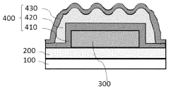
Flexible organic light-emitting diode (OLED) device of reduced stess at bending place and fabrication method thereof
PatentActiveUS11258038B2
Innovation
- A novel encapsulation layer configuration with a first and second inorganic layer and an organic layer, where the second inorganic layer has a continuous wavy curved configuration, formed by thermal stress differences, increasing contact area and reducing stress on the outer inorganic layer, and an optically clear adhesive is used to level the configuration.
Environmental Impact and Sustainability Considerations
The environmental impact of flexible OLED encapsulation technologies represents a critical consideration in the sustainable development of next-generation display technologies. Traditional encapsulation methods often rely on materials with significant ecological footprints, including energy-intensive glass production and environmentally persistent barrier films. The shift toward flexible OLED encapsulation presents both challenges and opportunities for improving the environmental profile of display manufacturing.
Material selection for flexible OLED encapsulation significantly influences sustainability outcomes. Thin-film encapsulation (TFE) approaches utilizing organic-inorganic hybrid materials can reduce raw material consumption compared to rigid glass alternatives. However, these advanced materials often incorporate rare earth elements or specialty chemicals that present extraction concerns and end-of-life management challenges. Recent innovations in bio-based barrier films and recyclable encapsulants show promise for reducing the environmental impact while maintaining optical clarity requirements.
Manufacturing processes for high-clarity flexible encapsulation typically demand precise deposition environments and significant energy inputs. Atomic Layer Deposition (ALD) and Plasma-Enhanced Chemical Vapor Deposition (PECVD), while effective for creating high-performance barriers, require substantial energy consumption and utilize greenhouse gas precursors. Industry leaders are exploring lower-temperature processes and alternative precursor chemistries to reduce the carbon footprint of these essential manufacturing steps.
The extended product lifecycle enabled by flexible, optically clear encapsulation technologies offers substantial sustainability benefits. Flexible OLEDs with effective encapsulation demonstrate greater resistance to mechanical failure, potentially extending device lifespans and reducing electronic waste generation. This durability factor must be balanced against the increased complexity of separating and recycling multi-layer barrier films at end-of-life.
Water and chemical usage in encapsulation processes presents another environmental consideration. Traditional approaches often require extensive cleaning steps and chemical treatments that generate wastewater containing trace metals and organic contaminants. Emerging dry encapsulation techniques and closed-loop manufacturing systems show potential for dramatically reducing water consumption and hazardous waste generation while maintaining the optical clarity demanded by premium display applications.
Regulatory frameworks worldwide are increasingly addressing the environmental aspects of electronics manufacturing, with particular focus on restricted substances and extended producer responsibility. Manufacturers pursuing advanced flexible OLED encapsulation must navigate evolving compliance requirements while designing for recyclability and reduced environmental impact. Industry consortia are developing standardized approaches to life cycle assessment specifically tailored to flexible display technologies, enabling more transparent environmental performance comparisons.
Manufacturing Scalability and Cost Analysis
The scalability of flexible OLED encapsulation technologies presents significant challenges for mass production implementation. Current thin-film encapsulation (TFE) processes require precise deposition of alternating inorganic and organic layers, with each layer demanding stringent control over thickness uniformity and defect density. Manufacturing yields for high-quality encapsulation remain below optimal levels, particularly as display sizes increase beyond 6 inches diagonal.
Production throughput represents a critical bottleneck, with typical encapsulation processes requiring 2-3 hours per batch using conventional equipment. Advanced atomic layer deposition (ALD) systems have improved cycle times to approximately 45 minutes, but still lag behind the rapid pace needed for cost-competitive manufacturing. The capital expenditure for establishing a production line capable of high-quality flexible OLED encapsulation exceeds $50-75 million, creating significant barriers to entry for smaller manufacturers.
Material costs constitute approximately 35-40% of total encapsulation expenses, with high-purity barrier materials commanding premium prices. Inorganic materials like aluminum oxide and silicon nitride cost $120-180 per kilogram, while specialized organic materials range from $300-500 per kilogram. Waste rates during deposition processes average 30-45%, substantially increasing effective material costs.
Energy consumption during vacuum deposition processes represents another significant cost factor, with typical encapsulation lines consuming 75-120 kWh per square meter of display area processed. Emerging plasma-enhanced chemical vapor deposition (PECVD) techniques have demonstrated potential energy reductions of 20-25%, but require substantial equipment modifications.
Quality control processes add further complexity and cost, with each encapsulation batch requiring comprehensive water vapor transmission rate (WVTR) testing. Current inline testing methods add approximately $0.75-1.25 per display unit to production costs. Defect detection systems capable of identifying sub-micron pinholes and delamination issues require investments of $2-3 million per production line.
Economic analysis indicates that encapsulation represents 15-22% of total flexible OLED manufacturing costs, with current technologies adding $8-12 per square foot to production expenses. Industry projections suggest that technological improvements and economies of scale could reduce these costs by 30-40% within the next three years, primarily through improved material utilization and faster deposition techniques. However, achieving the optical clarity targets while maintaining adequate moisture barriers will require continued investment in process optimization and equipment development.
Unlock deeper insights with PatSnap Eureka Quick Research — get a full tech report to explore trends and direct your research. Try now!
Generate Your Research Report Instantly with AI Agent
Supercharge your innovation with PatSnap Eureka AI Agent Platform!