Impact of Flexible OLED Encapsulation on Device Scalable Manufacturing
SEP 28, 20259 MIN READ
Generate Your Research Report Instantly with AI Agent
Patsnap Eureka helps you evaluate technical feasibility & market potential.
Flexible OLED Encapsulation Technology Evolution and Objectives
Flexible OLED (Organic Light-Emitting Diode) technology has evolved significantly over the past two decades, transforming from laboratory curiosity to commercial reality. The journey began in the early 2000s when researchers first demonstrated the potential of flexible organic displays. These early prototypes suffered from rapid degradation due to oxygen and moisture penetration, highlighting encapsulation as a critical challenge for commercialization.
The evolution of encapsulation technology can be traced through three distinct phases. The first phase (2000-2010) focused on glass-based rigid encapsulation, which provided excellent barrier properties but limited flexibility. During this period, researchers primarily explored multi-layer barrier films and early thin-film encapsulation (TFE) concepts.
The second phase (2010-2015) marked the transition to semi-flexible solutions, with hybrid approaches combining thin glass and barrier films. This period saw the emergence of atomic layer deposition (ALD) techniques for creating ultra-thin barrier layers with water vapor transmission rates (WVTR) below 10^-6 g/m²/day, a critical threshold for OLED longevity.
The current phase (2015-present) has been characterized by truly flexible encapsulation solutions, enabling foldable and rollable displays. Advanced TFE technologies combining inorganic and organic layers have become the industry standard, with major breakthroughs in plasma-enhanced chemical vapor deposition (PECVD) processes and organic-inorganic hybrid materials.
The primary objective of flexible OLED encapsulation technology is to achieve an optimal balance between barrier performance and mechanical flexibility while maintaining manufacturing scalability. Specifically, the industry aims to develop encapsulation solutions that can withstand repeated bending (>200,000 cycles at <3mm radius) while maintaining WVTR below 10^-6 g/m²/day and oxygen transmission rates below 10^-5 cc/m²/day.
Additional technical objectives include reducing encapsulation thickness to below 10μm to enhance overall device flexibility, extending operational lifetime to >50,000 hours under standard conditions, and developing processes compatible with high-throughput manufacturing (>80% yield at Gen 8+ substrate sizes).
From a manufacturing perspective, the industry is pursuing encapsulation technologies that can be integrated into existing production lines with minimal disruption, ideally utilizing roll-to-roll processing for cost reduction. There is also significant focus on developing environmentally sustainable encapsulation materials that reduce reliance on rare earth elements and minimize waste generation during manufacturing.
These technological objectives align with broader market demands for increasingly flexible, durable, and cost-effective display solutions across consumer electronics, automotive, and emerging wearable technology sectors.
Market Demand Analysis for Flexible OLED Displays
The flexible OLED display market has experienced remarkable growth in recent years, driven by increasing consumer demand for innovative form factors in electronic devices. Market research indicates that the global flexible OLED market reached approximately $12.3 billion in 2022 and is projected to grow at a compound annual growth rate (CAGR) of 27.4% through 2028, potentially reaching $53.8 billion by the end of the forecast period.
Consumer electronics, particularly smartphones, remain the primary driver of flexible OLED demand, accounting for over 65% of market share. Major smartphone manufacturers have increasingly adopted flexible OLED technology to enable foldable, rollable, and curved display designs that differentiate their premium product lines. The successful market reception of devices like Samsung's Galaxy Fold series and Motorola's Razr has validated consumer interest in these novel form factors.
Beyond smartphones, emerging application areas are expanding the market potential for flexible OLED displays. Wearable technology represents the fastest-growing segment, with smartwatches, fitness trackers, and augmented reality devices increasingly incorporating flexible displays. The automotive sector has also begun integrating flexible OLED panels in dashboard displays and entertainment systems, with luxury vehicle manufacturers leading adoption.
Regional analysis reveals Asia-Pacific as the dominant market for flexible OLED displays, accounting for approximately 58% of global demand. This concentration aligns with the region's manufacturing capabilities and consumer electronics ecosystem. North America and Europe follow with 22% and 15% market shares respectively, while showing accelerated growth rates as adoption expands beyond early adopters.
Consumer preference surveys indicate that device thinness, durability, and novel form factors are the primary drivers of flexible display appeal. However, price sensitivity remains a significant barrier to broader market penetration, with consumers expressing reluctance to pay premium prices for flexible display technology. This highlights the critical importance of scalable manufacturing solutions for flexible OLED encapsulation to reduce production costs.
Industry forecasts suggest that as encapsulation technologies mature and manufacturing yields improve, the price differential between rigid and flexible displays will narrow significantly by 2025. This cost reduction is expected to trigger a market inflection point, expanding flexible OLED adoption into mid-tier devices and accelerating market growth. Consequently, manufacturers who can solve scalable encapsulation challenges stand to capture substantial market share in this rapidly evolving landscape.
Current Encapsulation Techniques and Manufacturing Barriers
Flexible OLED encapsulation currently employs several key techniques, each with distinct manufacturing implications. Thin-film encapsulation (TFE) dominates the industry, utilizing alternating layers of inorganic and organic materials to create effective moisture and oxygen barriers. The inorganic layers (typically AlOx, SiNx, or SiOx) provide excellent barrier properties but are brittle, while organic layers (often acrylic polymers) offer flexibility and stress relief. This multi-layer approach creates a tortuous path for contaminants, significantly extending diffusion time.
Atomic Layer Deposition (ALD) represents a critical advancement in encapsulation technology, enabling the deposition of ultra-thin, highly conformal barrier layers with precise thickness control. However, ALD processes face significant throughput limitations due to their inherently slow deposition rates, creating a substantial manufacturing bottleneck for high-volume production.
Plasma-Enhanced Chemical Vapor Deposition (PECVD) offers higher throughput than ALD but struggles with achieving the same level of film quality and conformality on flexible substrates. The technique often produces films with higher defect densities, compromising barrier performance in flexible applications.
Roll-to-roll (R2R) processing presents a promising approach for continuous, high-throughput manufacturing but introduces complex technical challenges. Maintaining uniform deposition quality across large areas while handling flexible substrates remains problematic. Web handling issues, including substrate wrinkling and tension control, frequently lead to defects in the barrier layers.
A significant manufacturing barrier lies in particle contamination control. Even microscopic particles can create defect sites in thin barrier films, leading to localized barrier failures and device degradation. This challenge intensifies in flexible OLED production due to the handling of bendable substrates and the ultra-thin nature of the encapsulation layers.
Interface adhesion between different encapsulation layers presents another critical manufacturing challenge. Poor adhesion can lead to delamination during flexing, creating pathways for moisture ingress. Achieving strong interfacial bonding while maintaining flexibility requires precise surface treatments and material compatibility engineering.
Process integration complexity also impedes scalable manufacturing. The sequential deposition of multiple barrier layers demands careful coordination of various deposition technologies, often with different process requirements. Transitioning between these processes without compromising substrate integrity or introducing contamination requires sophisticated handling systems and environmental controls.
Yield management represents perhaps the most significant economic barrier. The stringent quality requirements for barrier films mean that even minor defects can render devices unusable. Current manufacturing processes struggle to achieve consistently high yields, particularly as substrate sizes increase, directly impacting production economics and commercial viability.
Current Scalable Manufacturing Solutions for Flexible OLEDs
01 Thin film encapsulation techniques for flexible OLEDs
Thin film encapsulation (TFE) is a critical technology for flexible OLEDs that involves depositing alternating inorganic and organic layers to create a barrier against moisture and oxygen. This approach enables the production of thin, flexible displays while maintaining effective protection of the sensitive OLED materials. The inorganic layers typically provide the barrier properties while the organic layers help with stress relief and flexibility. Advanced deposition techniques allow for precise control of layer thickness and uniformity, which is essential for scalable manufacturing.- Thin film encapsulation techniques for flexible OLEDs: Thin film encapsulation (TFE) is a key technology for flexible OLEDs that involves depositing alternating inorganic and organic layers to create a barrier against moisture and oxygen. This approach enables the production of thin, flexible displays while maintaining effective protection against environmental factors. The inorganic layers typically provide the barrier properties while the organic layers help with stress relief and flexibility. Advanced deposition techniques like atomic layer deposition (ALD) are used to create these thin films with precise thickness control.
- Roll-to-roll manufacturing processes for encapsulation: Roll-to-roll (R2R) manufacturing processes enable continuous, high-throughput production of flexible OLED encapsulation layers. This approach significantly improves scalability compared to batch processing methods. The technology involves unwinding a flexible substrate from one roll, processing it through various deposition stations for encapsulation layers, and rewinding the finished product onto another roll. This manufacturing method reduces production costs and increases throughput while maintaining consistent quality across large areas of flexible displays.
- Hybrid encapsulation systems combining inorganic and organic materials: Hybrid encapsulation systems utilize the complementary properties of both inorganic and organic materials to achieve optimal barrier performance for flexible OLEDs. Inorganic layers (such as silicon nitride, aluminum oxide) provide excellent barrier properties against moisture and oxygen, while organic layers (such as polymers) accommodate mechanical stress during bending. This multi-layer approach creates a tortuous path for permeants, significantly extending the lifetime of flexible OLEDs while maintaining the flexibility required for bendable displays.
- Low-temperature encapsulation processes for flexible substrates: Low-temperature encapsulation processes are essential for flexible OLEDs as they enable the use of temperature-sensitive polymer substrates. These techniques include plasma-enhanced chemical vapor deposition (PECVD), atomic layer deposition (ALD), and solution-based methods that can operate below 100°C. By avoiding high temperatures that would damage or deform flexible substrates, these processes allow for the mass production of flexible displays while maintaining the integrity of all device layers and the substrate.
- Edge sealing and mechanical protection for flexible displays: Edge sealing and mechanical protection technologies are critical for preventing lateral ingress of moisture and oxygen in flexible OLEDs. These approaches include specialized edge sealants, foldable edge protection structures, and integrated mechanical buffer layers that protect the active display area from physical damage during bending and folding operations. Advanced edge sealing techniques ensure complete encapsulation of the device while maintaining flexibility and preventing delamination during repeated mechanical stress cycles.
02 Roll-to-roll manufacturing processes for flexible OLED encapsulation
Roll-to-roll (R2R) manufacturing processes enable continuous, high-throughput production of flexible OLED encapsulation layers. This approach involves depositing barrier films onto flexible substrates as they move through various deposition stations. The continuous nature of R2R processing significantly increases production efficiency compared to batch processes, making it ideal for large-scale manufacturing. Key aspects include web handling systems, tension control, and synchronized deposition techniques that maintain uniform barrier properties across large areas while enabling cost-effective production of flexible OLEDs.Expand Specific Solutions03 Hybrid encapsulation systems combining inorganic and organic materials
Hybrid encapsulation systems utilize the complementary properties of inorganic and organic materials to create effective moisture barriers for flexible OLEDs. Inorganic layers (such as silicon nitride, aluminum oxide, or silicon oxide) provide excellent barrier properties, while organic layers (such as polymers or parylene) accommodate mechanical stress during flexing. This multilayer approach creates a tortuous path for moisture penetration while maintaining flexibility. Advanced deposition techniques allow for precise control of each layer's thickness and composition, optimizing both barrier performance and mechanical properties for flexible applications.Expand Specific Solutions04 Atomic layer deposition for high-quality barrier films
Atomic Layer Deposition (ALD) is a key technology for creating high-quality, pinhole-free barrier films for flexible OLED encapsulation. This technique enables the deposition of ultra-thin, conformal layers with precise thickness control at the atomic level. ALD processes can be optimized for large-area substrates and integrated into continuous manufacturing lines, making them suitable for scalable production. The resulting high-density films provide excellent protection against moisture and oxygen penetration while maintaining the flexibility required for bendable displays.Expand Specific Solutions05 Edge sealing and mechanical protection for flexible OLED devices
Edge sealing and mechanical protection are critical aspects of flexible OLED encapsulation that address vulnerability at device perimeters and during mechanical stress. Advanced edge sealing techniques prevent lateral moisture ingress at the boundaries of the encapsulation layers. Additional protective layers or films can be applied to enhance mechanical durability without compromising flexibility. These approaches include specialized adhesives, barrier edge structures, and composite materials that maintain barrier integrity during bending and folding while being compatible with high-volume manufacturing processes.Expand Specific Solutions
Leading Manufacturers and Industry Competitive Landscape
The flexible OLED encapsulation market is currently in a growth phase, with an estimated market size exceeding $2 billion and projected to expand significantly as demand for foldable displays increases. The technology maturity varies across key players, with Samsung Display and LG Display leading with advanced thin-film encapsulation technologies. Chinese manufacturers including BOE Technology, Tianma Microelectronics, and TCL China Star Optoelectronics are rapidly closing the gap through substantial R&D investments. The manufacturing scalability challenge remains significant, with companies like Visionox and Truly Semiconductors developing innovative approaches to barrier films and edge sealing techniques. The competitive landscape is characterized by intense patent activity and strategic partnerships between material suppliers and panel manufacturers to overcome yield and cost barriers.
BOE Technology Group Co., Ltd.
Technical Solution: BOE has developed a proprietary "Hybrid Barrier Multilayer" (HBM) encapsulation technology for flexible OLEDs, featuring alternating layers of inorganic barriers (primarily SiN and Al2O3) and organic buffer layers. Their manufacturing approach employs a combination of plasma-enhanced ALD for inorganic layers and vacuum thermal evaporation for organic materials. BOE's process achieves water vapor transmission rates of approximately 10^-5 g/m²/day while maintaining flexibility for radii down to 3mm. A key innovation in BOE's approach is their "selective area encapsulation" technique that applies different barrier structures to active and non-active areas of the display, optimizing both performance and manufacturing efficiency. Their Gen 6 flexible OLED lines incorporate in-line encapsulation systems capable of processing over 45,000 square meters of display area monthly, with reported yields approaching 80% for commercial products.
Strengths: Cost-effective manufacturing approach with selective area encapsulation reducing material usage; high production capacity with good yields; compatible with various flexible substrate materials. Weaknesses: Barrier performance slightly behind industry leaders; mechanical durability during repeated folding cycles needs improvement; relatively newer to mass production of flexible displays compared to Korean manufacturers.
Tianma Microelectronics Co., Ltd.
Technical Solution: Tianma has developed a "Gradient Hybrid Encapsulation" (GHE) technology for flexible OLEDs, featuring a novel approach where the composition of barrier layers gradually changes throughout the stack to optimize both barrier properties and mechanical flexibility. Their manufacturing process utilizes a combination of sputtering for inorganic layers and solution processing for organic materials, achieving water vapor transmission rates of approximately 5×10^-5 g/m²/day. Tianma's encapsulation technology incorporates a proprietary stress-distribution layer that enables reliable performance at bending radii of approximately 3-4mm through thousands of bending cycles. Their production implementation features a modular encapsulation system that can be configured for different product requirements, balancing performance and cost. Tianma has also developed specialized edge sealing techniques using laser-assisted deposition to address edge permeation issues in flexible displays.
Strengths: Highly adaptable manufacturing process suitable for various product specifications; good balance between performance and cost; innovative gradient barrier approach improves mechanical reliability. Weaknesses: Barrier performance not yet matching industry leaders; manufacturing throughput lower than top competitors; limited experience with ultra-thin flexible displays requiring extreme bending radii.
Key Patents and Innovations in Encapsulation Technology
Flexible organic light-emitting diode (OLED) device and fabrication method thereof
PatentActiveUS20210336206A1
Innovation
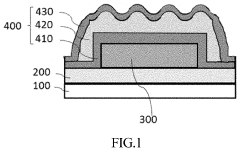
- A novel encapsulation layer configuration with a first and second inorganic layer and an organic layer, where the second inorganic layer has a continuous wavy curved configuration, increasing contact area and reducing stress, formed spontaneously due to thermal stress differences between layers.
OLED display panel and manufacturing method thereof
PatentActiveUS20210408443A1
Innovation
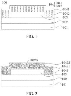
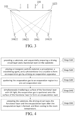
- An OLED display panel with a uniformly distributed inorganic particle material and organic material, where the inorganic particle material has a higher refractive index, is formed using an evaporation apparatus, where the inorganic particle material, pre-polymer, crosslinking agent, and photoinitiator are placed in crucibles to create a high-pressure gas, which is then sputtered onto the functional layer, optimizing the encapsulation layer's stability and transmittance by adjusting the evaporation rate ratios.
Cost-Benefit Analysis of Advanced Encapsulation Methods
The economic viability of advanced encapsulation methods for flexible OLED displays requires thorough cost-benefit analysis to determine their feasibility for mass production. Traditional encapsulation techniques using glass barriers and metal cans are cost-effective but incompatible with flexible display requirements, necessitating evaluation of newer approaches against manufacturing economics.
Thin-film encapsulation (TFE) technologies represent significant capital investment, with initial equipment costs ranging from $15-30 million per production line. However, these systems demonstrate superior throughput capabilities, processing 60-120 substrates per hour compared to 30-40 for conventional methods, potentially offsetting initial expenditures through improved production efficiency.
Material costs constitute another critical factor, with high-performance barrier films and inorganic-organic hybrid materials commanding premium prices of $50-100 per square meter. Despite higher material expenses, these advanced solutions deliver superior moisture barrier properties (water vapor transmission rates below 10^-6 g/m²/day), extending device lifetimes by 3-5 times compared to conventional approaches, thereby enhancing product value proposition.
Process complexity introduces additional cost considerations. Multi-layer encapsulation techniques require precise deposition control and specialized equipment, increasing production complexity and potential yield losses. Industry data suggests yield rates of 85-92% for advanced encapsulation processes compared to 94-97% for traditional methods, representing significant revenue impact at scale.
Energy consumption metrics reveal that atomic layer deposition (ALD) processes consume 2.5-3 times more energy than conventional PECVD methods, while plasma-enhanced ALD systems demonstrate 15-20% improved energy efficiency over thermal ALD alternatives. These operational costs accumulate substantially in high-volume manufacturing environments.
Long-term reliability benefits must be weighed against immediate production costs. Advanced encapsulation methods demonstrate mean time between failures (MTBF) improvements of 30-40% in accelerated aging tests, potentially reducing warranty claims and enhancing brand reputation. Market analysis indicates consumers willingly pay 15-25% premiums for devices with proven durability advantages.
Return on investment calculations suggest 2-3 year payback periods for advanced encapsulation technology investments, with economies of scale significantly improving cost structures as production volumes increase. Manufacturers achieving annual production volumes exceeding 5 million units report 30-40% reductions in per-unit encapsulation costs compared to initial production runs.
Environmental Impact and Sustainability Considerations
The manufacturing processes of flexible OLED encapsulation technologies present significant environmental challenges that must be addressed for sustainable industry development. Traditional encapsulation methods often involve environmentally harmful materials such as heavy metals and volatile organic compounds (VOCs), which pose risks to ecosystems and human health. The thin-film encapsulation (TFE) processes commonly used for flexible OLEDs require extensive energy consumption during deposition stages, contributing to the carbon footprint of manufacturing facilities.
Material waste represents another critical environmental concern in flexible OLED production. Current encapsulation techniques typically achieve yields of 70-85%, meaning substantial material wastage occurs during manufacturing. Additionally, the multi-layer barrier films often incorporate materials that are difficult to separate and recycle at end-of-life, creating downstream waste management challenges.
Water usage in encapsulation processes presents a growing sustainability concern, particularly in regions facing water scarcity. The cleaning and processing steps for high-precision barrier layers can consume significant quantities of ultra-pure water, with some manufacturing facilities reporting usage of 5-7 liters per square meter of display produced. Implementing closed-loop water recycling systems could reduce consumption by up to 60%, representing a significant opportunity for environmental improvement.
Energy efficiency innovations are emerging as potential solutions to reduce the environmental impact of encapsulation processes. Recent advancements in low-temperature plasma-enhanced chemical vapor deposition (PECVD) have demonstrated energy reductions of 30-40% compared to conventional methods while maintaining barrier performance. Similarly, atmospheric pressure deposition techniques are being developed to eliminate the need for energy-intensive vacuum systems.
The recyclability of flexible OLED components remains problematic due to the complex multi-material nature of encapsulation layers. Research into bio-based and biodegradable barrier materials shows promise, with some experimental formulations achieving moisture barrier properties approaching those of conventional materials while offering improved end-of-life characteristics. These materials could potentially reduce the environmental persistence of electronic waste.
Regulatory frameworks worldwide are increasingly focusing on the environmental impact of electronics manufacturing. The European Union's Restriction of Hazardous Substances (RoHS) directive and similar regulations in other regions are driving manufacturers toward greener encapsulation solutions. Companies demonstrating leadership in sustainable manufacturing practices are gaining competitive advantages through improved brand reputation and anticipation of stricter future regulations.
Unlock deeper insights with Patsnap Eureka Quick Research — get a full tech report to explore trends and direct your research. Try now!
Generate Your Research Report Instantly with AI Agent
Supercharge your innovation with Patsnap Eureka AI Agent Platform!