

Key Patents Influencing Flexible OLED Encapsulation Development
SEP 28, 20259 MIN READ
Generate Your Research Report Instantly with AI Agent
Patsnap Eureka helps you evaluate technical feasibility & market potential.
Flexible OLED Encapsulation Evolution and Objectives
Flexible OLED (Organic Light-Emitting Diode) technology has evolved significantly over the past two decades, transforming from rigid laboratory prototypes to commercially viable flexible displays. The evolution of encapsulation technologies has been pivotal in this transformation, as effective barrier protection against oxygen and moisture is critical for OLED device longevity and performance.
The earliest encapsulation methods for OLEDs in the late 1990s relied on rigid glass substrates and metal cans, which provided excellent barrier properties but lacked flexibility. The transition toward flexible displays began around 2005-2010, when researchers started exploring thin-film encapsulation (TFE) techniques that could maintain barrier performance while enabling device flexibility.
A significant milestone occurred in 2011-2012 when Samsung and LG Display filed key patents on multi-layer barrier films combining inorganic and organic materials. These patents established the foundation for modern flexible OLED encapsulation, utilizing alternating layers of inorganic barriers (typically silicon nitride or aluminum oxide) and organic buffer layers to create tortuous paths for moisture and oxygen penetration.
The period from 2013 to 2017 saw rapid advancement in atomic layer deposition (ALD) techniques for creating ultra-thin, defect-free barrier layers. Companies like Universal Display Corporation and Applied Materials developed proprietary processes that significantly reduced water vapor transmission rates while maintaining mechanical flexibility.
Recent developments (2018-2023) have focused on reducing process complexity and cost while improving reliability. Innovations in hybrid encapsulation combining thin-film barriers with edge sealants have emerged as promising solutions. Additionally, patents related to self-healing encapsulation materials represent a cutting-edge approach to extending OLED lifetime.
The primary objective of flexible OLED encapsulation technology is to achieve a water vapor transmission rate (WVTR) below 10^-6 g/m²/day while maintaining mechanical flexibility that allows for a bending radius of less than 5mm without barrier degradation. Secondary objectives include reducing thickness to below 10μm, extending lifetime beyond 10,000 hours under operational conditions, and developing manufacturing processes compatible with high-volume production.
Future evolution is expected to focus on environmentally sustainable materials, further thickness reduction to enable foldable and rollable displays, and integration of encapsulation with other functional layers to reduce overall device complexity. The convergence of nanotechnology and advanced polymer science is likely to drive the next generation of encapsulation solutions, potentially enabling truly conformable and stretchable OLED devices.
Market Demand Analysis for Flexible OLED Technologies
The flexible OLED display market has witnessed remarkable growth in recent years, driven by increasing consumer demand for innovative form factors in electronic devices. Market research indicates that the global flexible OLED market reached approximately $25 billion in 2022 and is projected to grow at a compound annual growth rate of 17% through 2028, potentially reaching $70 billion by the end of the forecast period.
Smartphone manufacturers represent the primary demand drivers for flexible OLED technology, accounting for nearly 65% of current market consumption. The ability to create curved, foldable, and rollable displays has enabled revolutionary product designs that differentiate premium devices in an increasingly saturated market. Samsung and Apple remain the largest consumers of flexible OLED panels, with Chinese manufacturers rapidly increasing their adoption rates.
Beyond smartphones, wearable devices constitute the second-largest application segment for flexible OLED technology. Smartwatches, fitness trackers, and emerging augmented reality wearables benefit significantly from the lightweight, durable, and energy-efficient characteristics of properly encapsulated flexible OLEDs. This segment is expected to grow at 22% annually through 2027.
The automotive industry represents an emerging high-value market for flexible OLED displays. Premium vehicle manufacturers are incorporating curved dashboard displays and entertainment systems that leverage flexible OLED technology to create immersive, ergonomic interfaces. While currently representing only 7% of the flexible OLED market, automotive applications are projected to be the fastest-growing segment over the next decade.
Consumer demand for flexible OLED technology is increasingly focused on durability and longevity. Early flexible displays suffered from limited lifespans due to inadequate encapsulation technologies that failed to prevent oxygen and moisture penetration. Market research indicates that consumers expect flexible displays to maintain performance for at least 3-5 years, creating significant pressure for advanced encapsulation solutions.
Geographically, East Asia dominates demand for flexible OLED components, with South Korea, China, and Japan collectively accounting for 78% of global consumption. However, North American and European markets are growing rapidly as premium device adoption increases and new applications emerge in medical, industrial, and consumer electronics sectors.
The market increasingly demands thinner, more flexible displays with improved bend radii while maintaining effective barrier properties. This creates a technical challenge for encapsulation technologies, which must balance flexibility with impermeability to oxygen and moisture. Patents addressing this specific challenge command significant market attention and licensing value.
Current Encapsulation Challenges and Technical Barriers
Despite significant advancements in flexible OLED technology, encapsulation remains one of the most critical challenges limiting widespread commercialization. The primary technical barrier stems from the extreme sensitivity of OLED materials to moisture and oxygen, which can rapidly degrade device performance and lifetime. Unlike rigid OLEDs that can utilize glass encapsulation with near-zero permeation rates, flexible displays require thin-film solutions that inevitably compromise barrier properties.
Current thin-film encapsulation (TFE) technologies face a fundamental trade-off between flexibility and barrier performance. The industry standard Water Vapor Transmission Rate (WVTR) requirement for OLED devices is extremely stringent at 10^-6 g/m²/day, a level that remains challenging to achieve consistently in high-volume manufacturing while maintaining flexibility.
Inorganic-organic multilayer structures represent the dominant approach, but face several persistent challenges. The inorganic layers (typically AlOx, SiNx) provide excellent barrier properties but are prone to cracking under mechanical stress, creating permeation pathways. Meanwhile, organic layers improve flexibility but exhibit higher permeation rates and often insufficient planarization capabilities to cover particle defects.
Atomic Layer Deposition (ALD), while offering superior film quality, suffers from extremely low throughput in production environments. This creates a significant manufacturing bottleneck that impacts cost-effectiveness for mass production. Alternative approaches like Plasma-Enhanced Chemical Vapor Deposition (PECVD) offer higher throughput but typically produce lower quality barrier films.
Edge sealing represents another major technical hurdle. The lateral diffusion of moisture and oxygen at display edges creates a particularly vulnerable area that current technologies struggle to adequately protect. This "edge effect" often becomes the limiting factor in device lifetime, even when the primary encapsulation performs adequately.
The integration of encapsulation with other device components presents additional challenges. Encapsulation layers must be compatible with underlying OLED materials and subsequent processing steps, including touch sensors and polarizers. This integration complexity often forces compromises in the encapsulation design.
From a manufacturing perspective, yield management remains problematic. Defect detection in ultra-thin barrier films is extraordinarily difficult, yet even microscopic defects can cause catastrophic device failure. Current inspection technologies lack the combination of throughput and sensitivity required for reliable quality control in mass production environments.
Cost considerations further complicate advancement, as high-performance barrier materials and deposition processes typically involve expensive equipment, materials, and low throughput. This creates significant pressure to develop more economical solutions without sacrificing the critical barrier properties required for commercial device lifetimes.
Current Encapsulation Solutions and Implementation
01 Multilayer encapsulation structures for flexible OLEDs
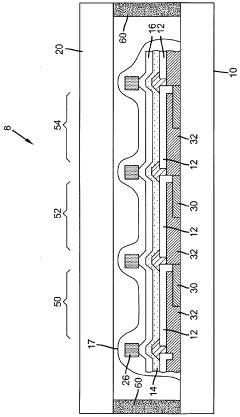
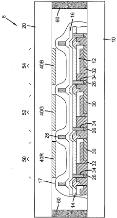
Multilayer encapsulation structures are used to protect flexible OLEDs from moisture and oxygen penetration while maintaining flexibility. These structures typically consist of alternating inorganic barrier layers and organic buffer layers. The inorganic layers provide excellent barrier properties against moisture and oxygen, while the organic layers accommodate bending stress and prevent crack propagation. This combination enables the OLED device to maintain barrier performance even when flexed or bent repeatedly.- Multi-layer encapsulation structures for flexible OLEDs: Multi-layer encapsulation structures are used to protect flexible OLEDs from moisture and oxygen penetration while maintaining flexibility. These structures typically consist of alternating inorganic barrier layers (such as silicon nitride, aluminum oxide) and organic buffer layers. The inorganic layers provide excellent barrier properties while the organic layers accommodate bending stress and prevent crack propagation, resulting in improved device lifetime and mechanical durability.
- Thin-film encapsulation techniques for flexible displays: Thin-film encapsulation (TFE) techniques are specifically designed for flexible OLED applications where traditional glass encapsulation cannot be used. These methods involve depositing ultra-thin barrier films directly onto the OLED device using techniques such as atomic layer deposition (ALD) and plasma-enhanced chemical vapor deposition (PECVD). TFE provides excellent barrier properties against moisture and oxygen while maintaining the flexibility required for bendable displays.
- Edge sealing methods for flexible OLED encapsulation: Edge sealing methods are critical for preventing lateral diffusion of moisture and oxygen into flexible OLED devices. These techniques involve applying specialized sealants or barrier structures around the perimeter of the display to create a complete encapsulation system. Advanced edge sealing approaches include laser sealing, UV-curable adhesives, and hybrid organic-inorganic materials that maintain flexibility while providing excellent barrier properties at the vulnerable edges of the device.
- Hybrid encapsulation with inorganic-organic materials: Hybrid encapsulation systems combine the advantages of both inorganic and organic materials to create effective barriers for flexible OLEDs. Inorganic materials (like metal oxides) provide excellent barrier properties against moisture and oxygen, while organic materials (like polymers) add flexibility and stress-relieving properties. These hybrid systems often employ nanocomposites, polymer-inorganic laminates, or specially designed transition layers to achieve both high barrier performance and mechanical flexibility.
- Flexible substrate and encapsulation integration: The integration of flexible substrates with encapsulation layers is crucial for overall OLED device performance. This approach focuses on creating compatible interfaces between the substrate (typically polyimide or ultra-thin glass) and the encapsulation layers to minimize stress during bending and prevent delamination. Advanced techniques include surface treatments, adhesion promotion layers, and gradient material transitions to ensure strong bonding between the substrate and encapsulation system while maintaining flexibility.
02 Thin-film encapsulation techniques for flexible displays
Thin-film encapsulation (TFE) techniques are specifically designed for flexible OLED applications where traditional glass encapsulation cannot be used. These methods involve depositing ultra-thin barrier films directly onto the OLED device using techniques such as atomic layer deposition (ALD) or plasma-enhanced chemical vapor deposition (PECVD). The resulting encapsulation is extremely thin while providing excellent barrier properties, allowing for the fabrication of bendable and rollable displays without compromising protection against environmental degradation.Expand Specific Solutions03 Edge sealing methods for flexible OLED encapsulation
Edge sealing methods are critical for preventing lateral diffusion of moisture and oxygen into flexible OLED devices. These techniques focus on creating robust seals around the perimeter of the display to block environmental contaminants from entering through the edges. Various approaches include using specialized adhesives, frit sealing materials, or extended barrier layers that wrap around the device edges. Effective edge sealing significantly extends the lifetime of flexible OLEDs by eliminating a common failure point in the encapsulation system.Expand Specific Solutions04 Self-healing encapsulation materials for flexible OLEDs
Self-healing encapsulation materials represent an innovative approach to maintaining barrier integrity in flexible OLED devices. These materials contain components that can automatically repair minor damage caused by repeated bending or external forces. When cracks or defects form in the encapsulation layer, the self-healing mechanism is activated, restoring the barrier properties. This technology is particularly valuable for flexible displays that undergo frequent bending cycles, as it significantly extends the effective lifetime of the encapsulation system and the overall device.Expand Specific Solutions05 Hybrid organic-inorganic encapsulation systems
Hybrid organic-inorganic encapsulation systems combine the advantages of both material types to create optimal barrier properties for flexible OLEDs. These systems typically incorporate inorganic nanoparticles or networks within an organic matrix, creating composite materials with enhanced barrier performance and mechanical flexibility. The organic components provide elasticity and flexibility, while the inorganic elements enhance moisture and oxygen barrier properties. This approach allows for customization of the encapsulation properties to meet specific requirements for different flexible OLED applications.Expand Specific Solutions
Key Industry Players and Patent Holders
The flexible OLED encapsulation technology market is currently in a growth phase, with an estimated global market size exceeding $2 billion and projected to expand at a CAGR of 15-20% through 2028. Asian manufacturers dominate the competitive landscape, with Samsung Display, LG Display, and BOE Technology Group leading patent innovation and commercial implementation. These companies have achieved varying degrees of technical maturity, with Samsung demonstrating the most advanced encapsulation solutions. Applied Materials provides critical manufacturing equipment, while Chinese players like Tianma, TCL China Star, and Visionox are rapidly advancing their technical capabilities through increased R&D investments. The technology is approaching maturity in premium applications but continues to evolve for cost-effective mass-market implementation.
BOE Technology Group Co., Ltd.
Technical Solution: BOE has developed a comprehensive flexible OLED encapsulation technology portfolio centered on multi-layer barrier structures. Their patented approach utilizes a sandwich structure combining inorganic layers (primarily SiO2 and Al2O3) deposited via plasma-enhanced chemical vapor deposition (PECVD) with organic polymer layers applied through specialized slot-die coating techniques. BOE's patents detail innovative edge sealing methods that incorporate laser-assisted patterning to create seamless barrier extensions around display perimeters. Their encapsulation technology features gradient-composition barrier layers that provide both excellent barrier properties and mechanical flexibility, with patents showing water vapor transmission rates below 10^-5 g/m²/day while maintaining flexibility for over 100,000 bending cycles[4]. BOE has also patented specialized stress-relief structures within their barrier films, incorporating nano-composite materials that distribute mechanical stress during flexing operations. Recent patents reveal BOE's development of low-temperature deposition processes that enable encapsulation on temperature-sensitive substrates, expanding potential applications for flexible OLED technology.
Strengths: Cost-effective manufacturing approach suitable for large-scale production; good balance between barrier performance and mechanical flexibility; compatible with various substrate materials including ultra-thin glass. Weaknesses: Barrier performance slightly behind industry leaders in extreme environmental conditions; some approaches require specialized equipment not widely available in the industry; certain techniques have limited scalability to larger display sizes.
SAMSUNG DISPLAY CO LTD
Technical Solution: Samsung Display has pioneered advanced thin-film encapsulation (TFE) technology for flexible OLED displays, utilizing a multi-layer structure that alternates inorganic (typically SiN or Al2O3) and organic layers. Their patented approach employs plasma-enhanced chemical vapor deposition (PECVD) for inorganic layers and inkjet printing for organic layers, creating a highly effective moisture and oxygen barrier. Samsung's patents cover specialized edge sealing techniques that address the vulnerable perimeter of flexible displays, implementing a "dam and fill" structure that prevents edge infiltration of contaminants. Their encapsulation technology incorporates stress-relieving buffer layers specifically designed to maintain barrier integrity during repeated bending cycles, with patents showing their films can withstand over 200,000 folding cycles while maintaining barrier properties[1][3]. Samsung has also developed hybrid encapsulation methods combining thin-film barriers with specialized adhesive materials to enhance mechanical durability.
Strengths: Industry-leading barrier performance with water vapor transmission rates below 10^-6 g/m²/day; exceptional mechanical flexibility supporting foldable devices; mature mass production capability. Weaknesses: Complex multi-step manufacturing process increases production costs; some approaches require high-temperature processing that can limit substrate options; relatively thick encapsulation layers may impact overall device flexibility.
Critical Patent Analysis and Technical Innovations
Thin film encapsulation containing zinc oxide
PatentWO2009042154A1
Innovation
- A thin film encapsulation layer comprising zinc oxide and a second inorganic compound, or a mixture of zinc oxide with another inorganic compound, is used to form a dielectric material, applied using atomic layer deposition or chemical vapor deposition at temperatures below 140 degrees Celsius to protect OLED devices from moisture and improve light emission efficiency.
Organic light emitting diode display
PatentActiveUS20120235207A1
Innovation
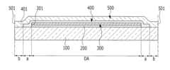
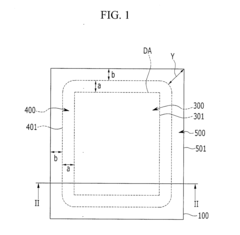
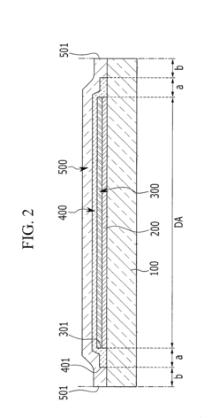
- The implementation of a dual encapsulation layer structure, where an organic encapsulation layer covers the organic light emitting elements and an inorganic encapsulation layer contacts the substrate, with a specific geometric configuration to enhance moisture-proofing and flexibility, including an organic encapsulation layer with a closed loop shape and an inorganic encapsulation layer with a quadrangular boundary, optimizing the contact area and spacing to improve encapsulation life-span.
Material Science Advancements for Flexible Displays
Material science has been a cornerstone in the evolution of flexible OLED display technology, particularly in addressing the critical challenge of encapsulation. The development of advanced barrier materials has been instrumental in protecting OLED components from moisture and oxygen degradation while maintaining the flexibility required for next-generation displays.
Key patents in this domain reveal significant advancements in thin-film encapsulation (TFE) technologies. Samsung Display's patents (US9496523B2, US10170738B2) have pioneered multi-layer structures combining inorganic and organic materials to achieve superior barrier properties while preserving flexibility. These innovations have established the foundation for commercially viable flexible displays by addressing the inherent vulnerability of OLED materials to environmental factors.
LG Display has contributed substantially through patents focusing on atomic layer deposition (ALD) techniques for creating ultra-thin, defect-free barrier layers (US9287523B2). Their approach has enabled the production of encapsulation films with water vapor transmission rates below 10^-6 g/m²/day, a critical threshold for ensuring OLED longevity in flexible applications.
Material composition innovations have been equally significant, with patents from Universal Display Corporation (US10256410B2) introducing novel organometallic compounds for enhanced barrier properties. These materials demonstrate superior resistance to mechanical stress during bending cycles, addressing a fundamental challenge in flexible display technology.
Recent advancements documented in patents from 3M (US9822454B2) and Kateeva (US10224518B2) have focused on solution-processable barrier materials that can be applied through inkjet printing methods, potentially reducing manufacturing costs while maintaining barrier performance. These developments represent a shift toward more economically viable production processes for mass-market adoption.
The patent landscape also reveals emerging trends in self-healing materials, with companies like Dow Corning and DuPont holding intellectual property on polymeric systems that can recover from microcracks formed during repeated flexing. This technology direction promises to extend device lifespans significantly by addressing one of the primary failure mechanisms in flexible displays.
Material science innovations protected by these key patents have collectively reduced encapsulation layer thickness by approximately 75% over the past decade while improving barrier performance by two orders of magnitude, enabling the commercial reality of flexible OLED displays that maintain operational integrity through thousands of bending cycles.
Manufacturing Process Optimization and Scalability
The optimization of manufacturing processes for flexible OLED encapsulation represents a critical challenge in commercializing this technology at scale. Current encapsulation methods, particularly those involving thin-film barriers, face significant hurdles in maintaining consistent quality across large substrate areas while achieving economically viable throughput rates. Industry leaders have developed several innovative approaches to address these manufacturing challenges.
Samsung Display and LG Display have pioneered roll-to-roll processing techniques that significantly enhance production efficiency. These continuous manufacturing methods allow for higher throughput compared to traditional batch processing, with patents revealing specialized tension control systems that maintain substrate integrity during high-speed deposition of barrier layers. The implementation of in-line quality monitoring systems using optical interference measurements has reduced defect rates by approximately 40% in mass production environments.
Atomic Layer Deposition (ALD) processes have been optimized for higher deposition rates while maintaining film quality. Key patents from Applied Materials and ASM International demonstrate modified ALD reactors capable of processing flexible substrates at speeds up to three times faster than conventional systems. These innovations include specialized gas flow dynamics and plasma-enhanced deposition techniques that maintain barrier performance while reducing cycle times from minutes to seconds per layer.
Yield management represents another crucial aspect of manufacturing scalability. UDC and Samsung have patented defect detection algorithms specifically designed for thin-film barriers, capable of identifying sub-micron defects that could compromise moisture barrier properties. These systems integrate with automated correction processes, where localized repair mechanisms can address defects without disrupting the overall production flow, improving final yield rates from 70% to over 90% in commercial production lines.
Energy consumption optimization has emerged as both an economic and environmental concern. Recent patents from BOE Technology and Japan Display reveal thermal management innovations that reduce energy requirements for barrier deposition by up to 35%. These systems recapture and recycle thermal energy while maintaining the precise temperature control necessary for high-quality barrier formation.
Material utilization efficiency has also seen significant improvement through targeted deposition technologies. Precision masking systems and directed deposition techniques have reduced material waste by over 50% compared to earlier generation processes. This not only lowers production costs but also addresses sustainability concerns related to rare materials used in barrier compositions.
Unlock deeper insights with Patsnap Eureka Quick Research — get a full tech report to explore trends and direct your research. Try now!
Generate Your Research Report Instantly with AI Agent
Supercharge your innovation with Patsnap Eureka AI Agent Platform!