Advanced Semiconductors in Microinjection Molding: A Comparative Study
OCT 15, 202510 MIN READ
Generate Your Research Report Instantly with AI Agent
PatSnap Eureka helps you evaluate technical feasibility & market potential.
Semiconductor Microinjection Molding Background and Objectives
Microinjection molding technology has evolved significantly over the past three decades, transforming from a niche manufacturing process to a cornerstone technology in semiconductor production. The integration of advanced semiconductor materials into microinjection molding represents a critical convergence of materials science and precision manufacturing. This technological evolution began in the early 1990s with basic polymer molding techniques and has progressively incorporated increasingly sophisticated semiconductor compounds and composites.
The semiconductor industry's relentless pursuit of miniaturization, following Moore's Law, has driven the development of microinjection molding processes capable of producing increasingly smaller and more complex components. This trajectory has been characterized by significant breakthroughs in material science, equipment precision, and process control methodologies. The historical progression shows a clear trend toward higher precision, greater material diversity, and enhanced functional integration.
Current technological trends indicate a growing emphasis on multi-material molding capabilities, particularly those involving advanced semiconductor materials such as silicon carbide (SiC), gallium nitride (GaN), and various polymer-semiconductor composites. These developments are enabling unprecedented levels of component integration and functionality within minimal form factors, essential for next-generation electronic devices.
The primary objective of this technical investigation is to conduct a comprehensive comparative analysis of various advanced semiconductor materials utilized in microinjection molding processes. This analysis aims to evaluate their respective performance characteristics, processing requirements, and suitability for specific applications across different industry sectors.
Secondary objectives include identifying optimal processing parameters for each material class, assessing the scalability of different semiconductor microinjection molding approaches, and determining cost-effectiveness metrics across various production volumes. Additionally, this research seeks to establish clear correlations between material properties, processing conditions, and final component performance.
The investigation will further explore emerging hybrid approaches that combine traditional microinjection molding with complementary technologies such as 3D printing, laser processing, and nanoimprint lithography. These hybrid methodologies represent potentially transformative approaches to semiconductor component manufacturing, offering new possibilities for geometric complexity and functional integration.
By establishing a comprehensive understanding of the current technological landscape and identifying promising development pathways, this research aims to provide valuable insights for strategic R&D investment decisions. The ultimate goal is to accelerate the adoption and optimization of advanced semiconductor microinjection molding technologies across relevant industrial applications, particularly in high-growth sectors such as medical devices, automotive electronics, and next-generation computing hardware.
Market Analysis for Advanced Semiconductor Molding Applications
The global market for advanced semiconductor molding applications is experiencing robust growth, driven by increasing demand for miniaturized electronic components across multiple industries. Current market valuations place this sector at approximately $12.5 billion, with projections indicating a compound annual growth rate of 7.8% through 2028. This growth trajectory is particularly evident in regions with established semiconductor manufacturing ecosystems, including East Asia, North America, and Western Europe.
Consumer electronics remains the dominant application segment, accounting for nearly 40% of market share. This is primarily due to the continuous evolution of smartphones, wearables, and portable computing devices that require increasingly sophisticated semiconductor packaging solutions. The automotive sector represents the fastest-growing segment, with demand increasing at approximately 9.3% annually as vehicles incorporate more advanced driver assistance systems, infotainment features, and electrification components.
Microinjection molding technologies specifically tailored for semiconductor applications have seen significant adoption in medical device manufacturing, where precision and biocompatibility are paramount. This segment currently represents about 15% of the total market but is expected to expand to 22% by 2027 as healthcare technologies become increasingly digitized and personalized.
Market analysis reveals a notable shift toward sustainable manufacturing processes within the semiconductor molding industry. Approximately 65% of major industry players have announced initiatives to reduce waste and energy consumption in their molding operations, responding to both regulatory pressures and consumer preferences for environmentally responsible products.
Supply chain considerations have become increasingly critical following recent global disruptions. The semiconductor molding application market has witnessed a 28% increase in regional manufacturing investments as companies pursue supply chain resilience through geographical diversification of production capabilities.
Customer demand patterns indicate growing preference for integrated solutions that combine advanced semiconductor materials with optimized molding processes. This trend has stimulated a 34% increase in collaborative research initiatives between material suppliers and molding technology providers over the past three years.
Price sensitivity varies significantly across application segments, with consumer electronics manufacturers demonstrating higher price elasticity compared to medical and aerospace sectors where performance and reliability considerations typically outweigh cost factors. This market dynamic has encouraged tiered product offerings from major suppliers, with premium solutions targeted at high-reliability applications and cost-optimized alternatives for consumer markets.
Current Technological Landscape and Challenges in Microinjection Molding
Microinjection molding technology has evolved significantly over the past decade, establishing itself as a critical manufacturing process for producing miniaturized components with high precision. Currently, the global landscape shows a mature technology in traditional polymer processing, while integration with advanced semiconductor materials represents an emerging frontier. Major manufacturing hubs in Germany, Japan, the United States, and increasingly China have developed specialized equipment capable of producing components with tolerances in the micrometer range and part weights below 1 mg.
The current technological infrastructure primarily consists of specialized microinjection units with shot volumes ranging from 0.05 to 5 cm³, utilizing screw diameters between 8 and 18 mm. These systems typically operate with injection pressures up to 3000 bar and injection speeds reaching 1000 mm/s to ensure complete filling of microcavities. Advanced process monitoring systems employing cavity pressure sensors and high-speed thermal imaging have become standard in high-end applications, particularly in semiconductor integration scenarios.
Despite these advancements, significant challenges persist in the microinjection molding of semiconductor materials. Material behavior at the micro-scale differs substantially from macro-scale processing, with surface tension effects, heat transfer dynamics, and flow characteristics presenting unique challenges. The high viscosity of semiconductor-polymer composites often leads to incomplete filling of micro-features, while rapid cooling rates can create residual stresses that compromise component integrity.
Tool design and fabrication represent another major hurdle, as mold features for semiconductor applications require sub-micron precision. Current micro-milling, laser ablation, and LIGA processes struggle to consistently achieve the necessary aspect ratios and surface finishes required for advanced semiconductor applications. Additionally, tool wear occurs more rapidly when processing semiconductor-filled compounds due to their abrasive nature.
Process control presents perhaps the most significant challenge, as the window for optimal processing parameters narrows dramatically at the micro-scale. Variations in temperature, pressure, or injection speed that would be negligible in conventional molding can lead to complete part failure in microinjection applications. This is particularly problematic when incorporating semiconductor materials with temperature-sensitive properties.
Quality assurance and metrology face limitations as well, with conventional inspection methods proving inadequate for the dimensional verification of microfeatures. Non-destructive testing methods capable of evaluating internal structures and semiconductor material distribution within polymer matrices remain underdeveloped, creating a significant bottleneck in production scaling.
The integration of semiconductor materials introduces additional complexities related to material compatibility, thermal management, and electrical performance preservation throughout the molding process. Current solutions often require trade-offs between processability and final semiconductor functionality, limiting widespread adoption in high-performance applications.
Comparative Analysis of Current Microinjection Molding Solutions
01 Advanced semiconductor manufacturing processes
Various advanced manufacturing processes have been developed to improve semiconductor production efficiency and quality. These include specialized etching techniques, deposition methods, and surface treatment processes that enhance the performance characteristics of semiconductor materials. These manufacturing innovations enable the production of smaller, more efficient semiconductor components with improved electrical properties and reliability.- Advanced semiconductor manufacturing processes: Various advanced manufacturing processes have been developed to improve semiconductor production efficiency and quality. These include specialized etching techniques, deposition methods, and surface treatment processes that enhance the performance characteristics of semiconductor materials. These manufacturing innovations enable the creation of more complex and miniaturized semiconductor devices with improved electrical properties and reliability.
- Semiconductor material innovations: Novel semiconductor materials and compositions have been developed to enhance device performance. These innovations include compound semiconductors, advanced silicon formulations, and specialized substrate materials that offer superior electrical, thermal, and mechanical properties compared to traditional semiconductors. These materials enable the development of high-performance electronic devices with improved efficiency and functionality.
- Semiconductor device structures and architectures: Advanced semiconductor device architectures incorporate innovative structural designs to improve performance and functionality. These include three-dimensional structures, novel transistor configurations, and integrated circuit layouts that optimize electron flow and reduce power consumption. These architectural innovations enable higher integration density and improved performance in modern electronic systems.
- Semiconductor packaging and integration technologies: Advanced packaging and integration technologies have been developed to improve semiconductor device performance and reliability. These include novel interconnection methods, thermal management solutions, and multi-chip integration approaches that enhance signal integrity and reduce form factors. These packaging innovations enable the development of more compact and efficient electronic systems with improved thermal and electrical characteristics.
- Semiconductor applications in emerging technologies: Advanced semiconductors are being applied in various emerging technology fields, including quantum computing, artificial intelligence hardware, and advanced sensing systems. These applications leverage specialized semiconductor properties to enable new functionalities and performance levels not possible with conventional electronics. The integration of advanced semiconductors in these emerging fields is driving innovation across multiple industries and creating new technological capabilities.
02 Semiconductor material innovations
Novel semiconductor materials and compositions have been developed to enhance device performance. These innovations include compound semiconductors, advanced silicon formulations, and specialized substrate materials that offer improved electrical conductivity, thermal stability, and other desirable properties. These material innovations enable the creation of semiconductor devices with superior performance characteristics for various applications.Expand Specific Solutions03 Semiconductor device structures and architectures
Advanced semiconductor device structures and architectures have been designed to improve performance and functionality. These include novel transistor designs, integrated circuit layouts, and three-dimensional semiconductor structures that enhance processing capabilities while reducing power consumption. These architectural innovations enable the development of more powerful and energy-efficient electronic systems.Expand Specific Solutions04 Semiconductor packaging and integration technologies
Advanced packaging and integration technologies have been developed to improve semiconductor device performance and reliability. These include specialized encapsulation methods, interconnect technologies, and thermal management solutions that enhance the protection and functionality of semiconductor components. These packaging innovations enable the creation of more compact, reliable, and thermally efficient semiconductor devices.Expand Specific Solutions05 Semiconductor applications in emerging technologies
Advanced semiconductors are being applied in various emerging technology fields. These applications include use in quantum computing, artificial intelligence processors, advanced sensors, and next-generation communication systems. These semiconductor innovations enable the development of cutting-edge technologies that address complex computational challenges and enable new capabilities in various industries.Expand Specific Solutions
Leading Companies and Research Institutions in the Field
The microinjection molding semiconductor market is currently in a growth phase, characterized by increasing demand for miniaturized components in electronics and medical devices. The market is projected to expand significantly due to advancements in semiconductor integration with molding technologies. Leading players include established semiconductor giants like TSMC, Samsung Electronics, and GlobalFoundries, who possess advanced manufacturing capabilities. SMIC and Huawei represent China's growing influence in this sector. IBM and Renesas contribute significant intellectual property and specialized solutions. The technology maturity varies, with companies like NXP and Mitsubishi Electric focusing on application-specific innovations, while research institutions like Xi'an Jiaotong University and Guangzhou University collaborate with industry to bridge theoretical and practical gaps. The competitive landscape reflects a blend of established manufacturers and emerging specialized providers.
Samsung Electronics Co., Ltd.
Technical Solution: Samsung has developed a comprehensive semiconductor microinjection molding platform focused on advanced packaging solutions for memory and logic devices. Their technology employs multi-material injection molding systems that can process high-performance thermoplastics with embedded metallic components for enhanced electrical and thermal conductivity. Samsung's approach features precision temperature-controlled mold cavities that maintain tolerances within ±5μm across complex geometries. The company has integrated real-time monitoring systems using embedded sensors to track material flow, pressure distribution, and curing parameters during the molding process. This data-driven approach enables adaptive process control, significantly reducing defect rates to below 10 parts per million for their most advanced packages. Samsung has also pioneered the use of liquid crystal polymer (LCP) materials in semiconductor microinjection molding, offering superior mechanical stability and electrical performance at frequencies above 5GHz, critical for 5G and next-generation wireless applications.
Strengths: Vertical integration allowing for customized material formulations; extensive experience with high-volume manufacturing; advanced process monitoring and quality control systems. Weaknesses: Higher capital investment requirements; complex setup procedures for new product introductions; challenges with ultra-thin wall sections below 50μm.
Merck Patent GmbH
Technical Solution: Merck has focused on developing specialized materials and process technologies for semiconductor microinjection molding applications. Their portfolio includes engineered thermoplastic compounds with precisely controlled electrical properties, ranging from highly insulating (volume resistivity >10^16 Ω·cm) to selectively conductive materials that can be tailored for specific semiconductor applications. The company has pioneered the development of liquid crystal polymer (LCP) formulations with exceptional dimensional stability (coefficient of thermal expansion <8 ppm/°C) and moisture absorption below 0.04%, critical for maintaining the integrity of semiconductor packages in challenging environments. Merck's microinjection molding technology incorporates specialized additives that enhance flow characteristics while maintaining molecular orientation, achieving aspect ratios exceeding 200:1 in microfeatures. Their materials science approach includes the development of thermally conductive polymers with conductivity values up to 15 W/m·K without compromising electrical insulation properties. Recent innovations include photopatternable polymers that can be selectively cured post-molding, enabling the creation of complex three-dimensional electrical interconnects within semiconductor packages.
Strengths: Unparalleled materials science expertise; ability to customize material properties for specific applications; strong intellectual property portfolio in specialized polymer formulations. Weaknesses: Reliance on manufacturing partners for implementation; limited direct control over molding processes; higher material costs compared to standard compounds.
Key Patents and Technical Innovations in Semiconductor Microinjection
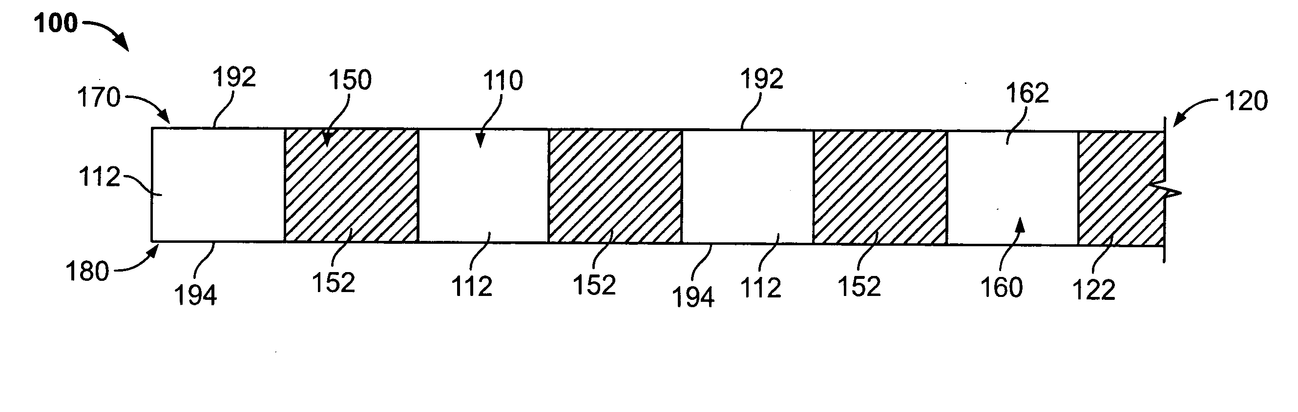
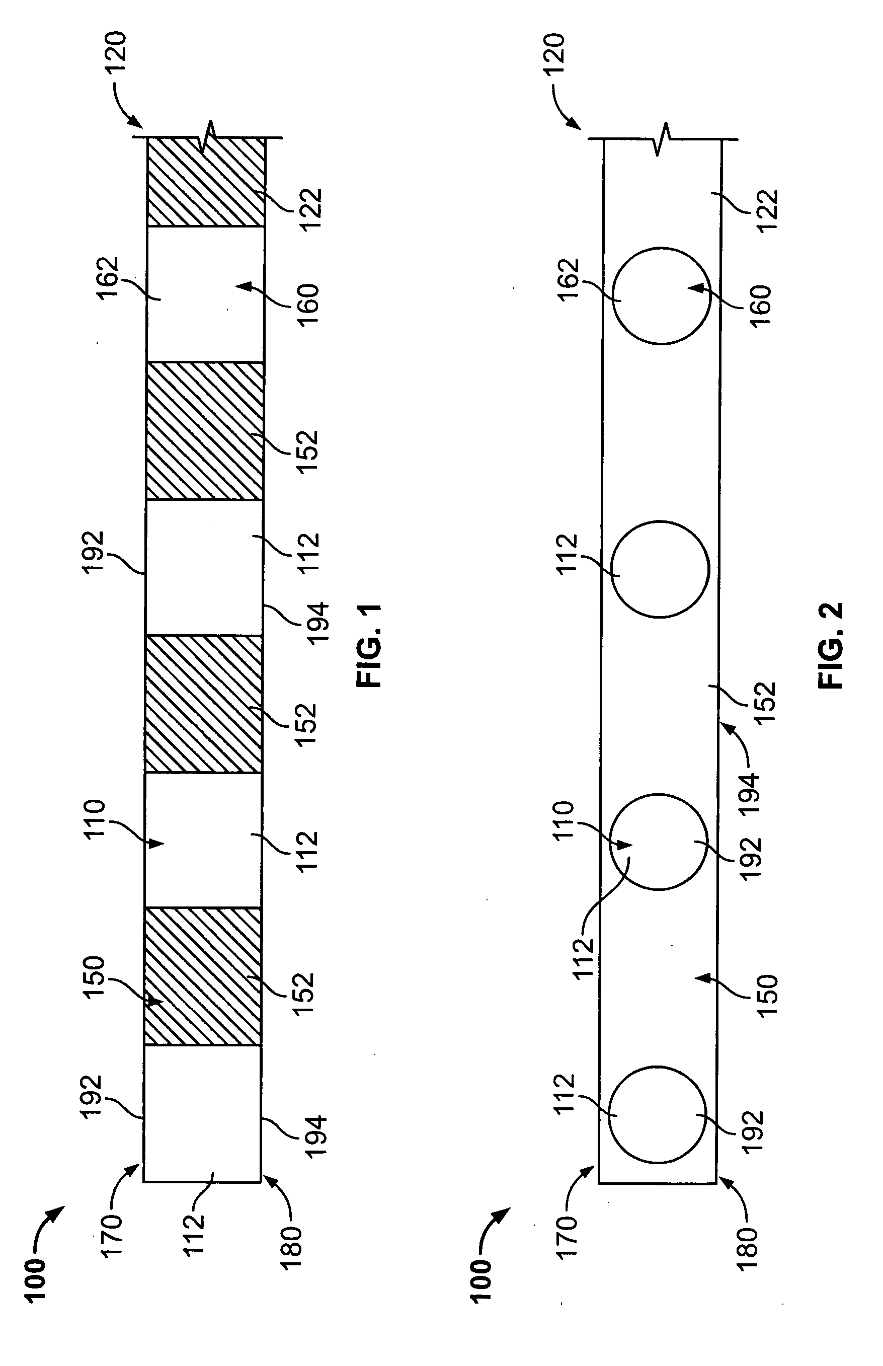
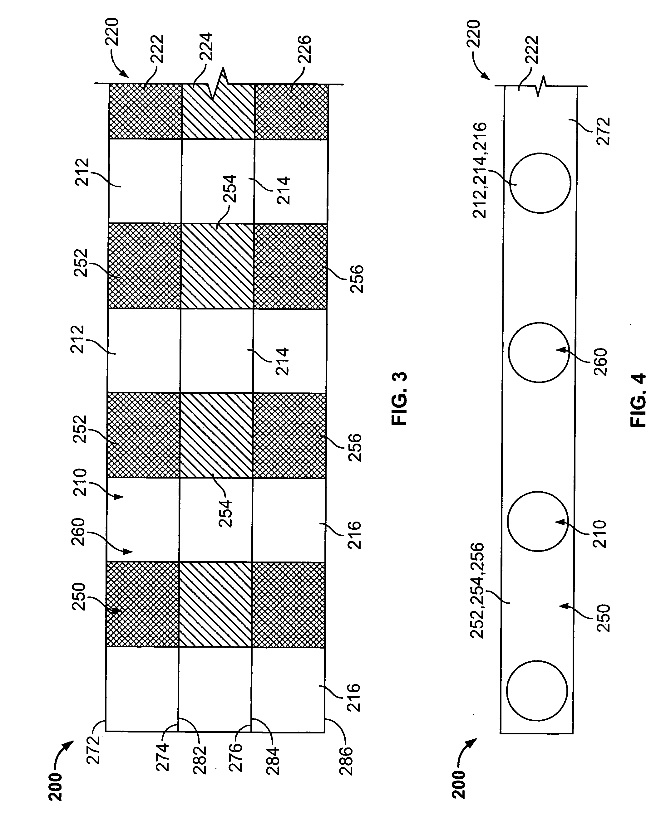
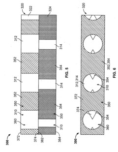
System and method of micromolded filtration microstructure and devices
PatentInactiveUS20070151920A1
Innovation
- The use of injection micromolding technology with advanced tool micro-machining techniques like EDM, MEDM, or laser beam machining to create precise filtration microstructures with a one-shot or multi-shot molding process, allowing for the production of filters with varying channel configurations and rigid structures that maintain consistency and efficiency.
Supercritical fluid microcellular injection molding equipment and injection molding method thereof
PatentInactiveUS20190091901A1
Innovation
- The method involves preheating a feed pipe to a hot melt temperature, injecting supercritical fluid into a metering screw that mixes with hot molten polymer, and using a combination of first and second gear pumps to maintain discharge rate and reduce pressure, resulting in uniform microbubbles and eliminating surface wrinkles through controlled depressurization and cooling.


Material Science Advancements for Semiconductor Microinjection
Recent advancements in material science have revolutionized semiconductor microinjection molding processes, enabling unprecedented precision and functionality in microelectronic components. The evolution of semiconductor materials specifically designed for microinjection applications has progressed significantly over the past decade, with particular emphasis on thermal stability, flow characteristics, and electrical performance.
Silicon-based compounds have undergone substantial refinement, with the introduction of high-purity polysilicon formulations that demonstrate superior moldability while maintaining essential semiconductor properties. These advanced materials exhibit glass transition temperatures optimized for the microinjection process window, allowing for more precise control during the molding phase without compromising electrical characteristics.
Polymer-semiconductor composites represent another breakthrough category, incorporating nanoscale semiconductor particles within specialized polymer matrices. These materials offer unique advantages in terms of processability and cost-effectiveness while providing customizable electrical and thermal conductivity profiles. Recent developments have focused on improving the interface between polymer and semiconductor components to enhance overall performance and reliability.
Metal-organic frameworks (MOFs) adapted for semiconductor applications have emerged as promising candidates for specialized microinjection applications. These materials feature precisely engineered porous structures that can be tailored at the molecular level, offering unprecedented control over electrical properties while maintaining compatibility with standard microinjection equipment and processes.
Thermal management innovations have addressed one of the most significant challenges in semiconductor microinjection molding. New composite materials incorporating diamond nanoparticles and carbon nanotubes demonstrate thermal conductivity values approaching those of bulk copper while maintaining the flow characteristics necessary for successful microinjection processes. These advancements have enabled the production of increasingly miniaturized components with improved heat dissipation capabilities.
Surface modification technologies have similarly evolved to enhance the interface between molded semiconductor materials and additional components. Plasma-assisted treatments and specialized coupling agents now allow for improved adhesion and electrical contact between dissimilar materials, expanding design possibilities for complex microelectronic systems.
Biodegradable semiconductor materials represent an emerging frontier, responding to increasing environmental concerns and regulatory pressures. These materials incorporate organic semiconductor compounds within biodegradable polymer matrices, offering potential solutions for temporary electronic applications and reducing electronic waste while maintaining compatibility with existing microinjection molding infrastructure.
The integration of 2D materials such as graphene and transition metal dichalcogenides into injection-moldable formulations has opened new possibilities for flexible and transparent semiconductor components. These materials offer exceptional electrical properties combined with mechanical flexibility that traditional semiconductor materials cannot match, enabling novel form factors and applications previously unattainable through conventional microinjection molding techniques.
Environmental Impact and Sustainability Considerations
The integration of advanced semiconductors in microinjection molding processes presents significant environmental and sustainability considerations that must be addressed as this technology advances. The manufacturing of semiconductor components traditionally involves substantial resource consumption, including high energy usage, water consumption, and the utilization of potentially hazardous chemicals. When these advanced materials are incorporated into microinjection molding processes, the environmental footprint becomes a complex interplay of multiple manufacturing stages.
Energy efficiency represents a critical environmental factor in semiconductor-enhanced microinjection molding. The production of advanced semiconductor materials requires precision-controlled environments with substantial energy demands for maintaining cleanrooms, operating high-temperature processes, and powering specialized equipment. However, recent innovations have demonstrated potential for reducing energy consumption through optimized process parameters and equipment designs specifically tailored for semiconductor-polymer integration.
Material selection and waste management constitute another significant environmental consideration. The semiconductor industry has historically relied on rare earth elements and potentially toxic materials. When these are incorporated into microinjection molded products, end-of-life considerations become increasingly complex. Research indicates that advanced design approaches focusing on material compatibility can facilitate more effective recycling and recovery of valuable semiconductor components from discarded products.
Water usage in semiconductor manufacturing for microinjection applications presents both challenges and opportunities for sustainability improvements. Traditional semiconductor fabrication processes are water-intensive, often requiring ultra-pure water for cleaning and processing. Emerging closed-loop water recycling systems specifically designed for integrated semiconductor-polymer manufacturing have demonstrated potential water usage reductions of 30-45% compared to conventional approaches.
Carbon footprint assessments of advanced semiconductor microinjection molding reveal that transportation impacts can be minimized through localized production strategies. The miniaturization enabled by these technologies allows for more compact manufacturing facilities that can be strategically positioned closer to end markets, reducing emissions associated with global supply chains.
Regulatory compliance and evolving environmental standards are increasingly shaping the development trajectory of semiconductor-enhanced microinjection molding. The European Union's Restriction of Hazardous Substances (RoHS) directive, along with similar regulations worldwide, has accelerated research into alternative materials and processes that maintain performance while reducing environmental impact. Companies leading in this field have begun implementing comprehensive life cycle assessments to quantify and minimize environmental impacts across the entire product lifecycle.
Unlock deeper insights with PatSnap Eureka Quick Research — get a full tech report to explore trends and direct your research. Try now!
Generate Your Research Report Instantly with AI Agent
Supercharge your innovation with PatSnap Eureka AI Agent Platform!