

Analysis of Chiplet Integration for Semiconductor Standardization
OCT 15, 20259 MIN READ
Generate Your Research Report Instantly with AI Agent
PatSnap Eureka helps you evaluate technical feasibility & market potential.
Chiplet Technology Evolution and Objectives
The evolution of chiplet technology represents a paradigm shift in semiconductor design and manufacturing, moving away from monolithic system-on-chip (SoC) architectures toward modular, disaggregated approaches. This transition began in the early 2010s when traditional semiconductor scaling following Moore's Law encountered significant physical and economic barriers. The increasing costs of advanced node manufacturing and the diminishing returns of transistor scaling prompted the industry to explore alternative integration strategies.
Chiplet technology emerged as a solution that allows different functional blocks to be manufactured separately using optimal process nodes, then integrated onto a common substrate. This approach enables heterogeneous integration, combining components fabricated with different technologies while maintaining high-performance interconnects between them. The evolution has progressed from simple multi-chip modules to sophisticated 2.5D and 3D integration schemes utilizing advanced packaging technologies.
The primary objective of chiplet technology development is to overcome the limitations of monolithic integration while maintaining or improving system performance, power efficiency, and cost-effectiveness. By disaggregating complex SoCs into smaller, more manageable chiplets, manufacturers can achieve higher yields, reduce development costs, and accelerate time-to-market for new products. Additionally, chiplet-based designs offer greater flexibility and reusability, allowing companies to mix and match pre-validated IP blocks.
Standardization represents a critical milestone in chiplet technology evolution. Early implementations were predominantly proprietary solutions developed by individual companies. However, the industry has recognized that widespread adoption requires standardized interfaces and protocols to enable interoperability between chiplets from different vendors. Organizations such as JEDEC, OCP, and CHIPS Alliance have initiated efforts to develop open standards for chiplet interfaces, testing methodologies, and design frameworks.
The technology trajectory indicates a clear trend toward more sophisticated integration schemes, with increasing emphasis on high-bandwidth, low-latency die-to-die interconnects. Advanced packaging technologies like silicon interposers, embedded bridge technologies, and direct copper bonding continue to evolve alongside chiplet designs, enabling ever-closer integration of disparate components.
Looking forward, the objectives for chiplet technology include establishing comprehensive industry standards, reducing integration costs, improving thermal management, and enhancing security features for multi-vendor chiplet ecosystems. The ultimate goal is to create a vibrant marketplace where chiplets from various suppliers can be seamlessly integrated, fostering innovation and competition while addressing the technical and economic challenges facing the semiconductor industry.
Market Demand Analysis for Chiplet Solutions
The chiplet market is experiencing unprecedented growth driven by several converging factors in the semiconductor industry. As traditional monolithic chip designs face increasing challenges in maintaining Moore's Law progression, chiplet-based architectures have emerged as a compelling alternative. Current market analysis indicates that the global chiplet market is projected to grow at a compound annual growth rate of 40% between 2023 and 2028, reaching approximately 50 billion dollars by the end of this period.
This remarkable growth is primarily fueled by escalating demand for high-performance computing solutions across multiple sectors. Data centers and cloud service providers are increasingly adopting chiplet-based designs to address their requirements for enhanced computational power while managing thermal constraints and energy consumption. The hyperscaler market segment has shown particular interest in chiplet solutions, with major players like Google, Amazon, and Microsoft actively investing in this technology to optimize their server infrastructure.
Consumer electronics represents another significant market driver, as smartphones, tablets, and other personal devices require increasingly sophisticated processing capabilities within strict power and space limitations. The automotive sector is similarly emerging as a key growth area, with advanced driver-assistance systems and autonomous driving technologies demanding unprecedented computational performance in vehicle-compatible form factors.
From a geographical perspective, North America currently leads chiplet adoption, accounting for approximately 45% of the market share, followed by Asia-Pacific at 35% and Europe at 20%. However, the Asia-Pacific region is expected to demonstrate the fastest growth rate over the next five years due to substantial investments in semiconductor manufacturing infrastructure in countries like Taiwan, South Korea, and China.
Market research indicates that standardization is becoming a critical factor influencing adoption rates. A recent industry survey revealed that 78% of potential chiplet technology adopters consider standardization essential for their implementation decisions. The lack of unified standards currently represents a significant barrier to wider market penetration, with interoperability concerns cited by 65% of surveyed companies as a major obstacle to chiplet adoption.
Cost considerations also play a pivotal role in market dynamics. While chiplet designs offer potential cost advantages through improved yield and die reuse, the current integration and packaging expenses partially offset these benefits. Market analysis suggests that standardization could reduce these integration costs by up to 30%, potentially accelerating adoption across price-sensitive market segments such as consumer electronics and industrial applications.
Current Chiplet Integration Challenges
Despite significant advancements in chiplet technology, the semiconductor industry faces several critical integration challenges that impede standardization efforts. The most pressing issue remains the lack of universal interconnect standards, with competing protocols like UCIe, BoW, and AIB creating market fragmentation. This heterogeneity forces designers to make early architectural commitments that limit flexibility and increase development costs.
Physical integration presents substantial technical hurdles, particularly in achieving precise die-to-die alignment at microscopic scales. Current manufacturing processes struggle with thermal expansion mismatches between materials, creating reliability concerns for high-density interconnects. These challenges are exacerbated as interconnect pitches continue to shrink below 40 microns, pushing the boundaries of existing assembly technologies.
Testing methodologies represent another significant obstacle. Unlike traditional monolithic designs, chiplet-based systems require sophisticated Known-Good-Die (KGD) testing protocols to ensure each component functions correctly before integration. The industry lacks standardized approaches for this critical step, resulting in yield losses and increased production costs. Post-integration testing becomes exponentially more complex as the number of chiplets increases, creating a verification bottleneck.
Power delivery and thermal management present formidable engineering challenges. Current solutions struggle to efficiently distribute power across multiple chiplets while maintaining signal integrity. Thermal hotspots at interconnect boundaries can significantly impact system reliability and performance, particularly in high-performance computing applications where power densities continue to increase.
The ecosystem fragmentation extends beyond technical specifications to business models. Intellectual property protection, licensing frameworks, and supply chain integration remain underdeveloped for chiplet-based designs. Without standardized approaches to these business considerations, companies hesitate to fully commit to chiplet strategies, slowing industry-wide adoption.
Data security and integrity concerns emerge as chiplets from different vendors are integrated into single packages. The industry lacks robust verification methodologies to ensure chiplets from various sources can securely interact without compromising system integrity or exposing sensitive information across die boundaries.
Software development tools and design automation solutions for chiplet-based systems remain immature compared to traditional SoC workflows. EDA vendors are still evolving their offerings to address the unique challenges of multi-die integration, creating a toolchain gap that increases design complexity and time-to-market.
Current Chiplet Integration Architectures
01 Standardized Chiplet Interfaces and Protocols
Standardized interfaces and protocols are essential for chiplet integration, enabling different chiplets from various manufacturers to communicate effectively. These standards define electrical signaling, physical connections, and communication protocols that ensure interoperability between chiplets. Standardization efforts focus on creating universal interfaces that support high-bandwidth, low-latency connections while maintaining power efficiency across heterogeneous chiplet designs.- Standardized Interfaces for Chiplet Integration: Standardized interfaces are crucial for chiplet integration, enabling different chiplets from various manufacturers to communicate effectively. These interfaces define protocols, signaling standards, and physical connections between chiplets, facilitating interoperability across the semiconductor ecosystem. Standardization efforts focus on creating common specifications for die-to-die connections, ensuring compatibility and reducing integration challenges in heterogeneous systems.
- Advanced Packaging Technologies for Chiplet Integration: Advanced packaging technologies enable effective chiplet integration by providing the physical infrastructure for connecting multiple dies. These technologies include interposers, bridge chips, and through-silicon vias (TSVs) that facilitate high-bandwidth, low-latency communication between chiplets. Standardization in packaging approaches ensures consistent thermal management, power delivery, and signal integrity across different chiplet-based designs, supporting the broader adoption of modular semiconductor architectures.
- Testing and Validation Standards for Chiplet Systems: Standardized testing and validation methodologies are essential for ensuring the reliability and performance of chiplet-based systems. These standards define procedures for pre-integration testing of individual chiplets, as well as post-integration validation of complete systems. By establishing common testing protocols, manufacturers can ensure interoperability between chiplets from different sources and verify compliance with performance specifications, reducing integration risks and accelerating time-to-market.
- Power Management and Thermal Standards for Chiplet Designs: Standardized approaches to power management and thermal control are critical for chiplet integration, particularly as system complexity increases. These standards define common methodologies for power delivery, voltage regulation, and thermal dissipation across chiplet interfaces. By establishing uniform power and thermal specifications, designers can ensure reliable operation of heterogeneous chiplet systems while optimizing energy efficiency and preventing thermal issues that could affect performance or reliability.
- Industry Consortia and Collaborative Standardization Efforts: Industry consortia play a vital role in developing and promoting chiplet integration standards through collaborative efforts among semiconductor companies, equipment manufacturers, and research institutions. These organizations work to establish open standards that benefit the entire ecosystem, addressing challenges in interoperability, design methodologies, and manufacturing processes. Collaborative standardization initiatives help accelerate the adoption of chiplet technology by creating common frameworks that enable innovation while ensuring compatibility across the industry.
02 Advanced Packaging Technologies for Chiplet Integration
Advanced packaging technologies are crucial for effective chiplet integration, including 2.5D and 3D integration approaches. These technologies involve interposers, through-silicon vias (TSVs), and micro-bumps that enable high-density connections between chiplets. Standardized packaging methodologies ensure thermal management, mechanical stability, and reliable electrical connections while supporting heterogeneous integration of chiplets with different process technologies.Expand Specific Solutions03 Chiplet Design and Testing Standards
Standardized design and testing methodologies for chiplets ensure quality, reliability, and compatibility across the ecosystem. These standards include pre-silicon verification, post-silicon validation, and known-good-die testing protocols specific to chiplet architectures. Design standards encompass power domains, clock distribution, thermal considerations, and physical form factors that facilitate integration while maintaining performance and yield requirements.Expand Specific Solutions04 Chiplet Ecosystem and IP Management
Standardization of chiplet ecosystems involves intellectual property management, business models, and supply chain considerations. These standards define how chiplet IP can be licensed, integrated, and verified across multiple vendors. The ecosystem standards address chiplet catalogs, marketplace frameworks, and quality assurance methodologies that enable semiconductor companies to collaborate effectively while protecting their intellectual property and ensuring consistent quality.Expand Specific Solutions05 Chiplet Power and Thermal Management Standards
Power and thermal management standards for chiplets address the unique challenges of heterogeneous integration. These standards define power delivery networks, thermal interface materials, and cooling solutions specific to multi-chiplet designs. Standardized approaches to power states, thermal monitoring, and dynamic power management ensure reliable operation while maximizing performance and energy efficiency across chiplets with different process technologies and power requirements.Expand Specific Solutions
Key Industry Players in Chiplet Ecosystem
The chiplet integration market for semiconductor standardization is currently in a growth phase, with increasing adoption across the industry. The market is expanding rapidly, driven by the need for more efficient and cost-effective semiconductor solutions, with projections suggesting significant growth over the next five years. Technologically, the field is maturing with major players like TSMC, Samsung, and Intel leading innovation. TSMC and Samsung have established advanced chiplet integration capabilities, while companies like AMD have successfully commercialized chiplet-based products. Emerging players such as Chipletz are developing specialized integration solutions. Asian manufacturers including SMIC and SK hynix are investing heavily in this technology, while established semiconductor companies like IBM and Sony are incorporating chiplet approaches into their product roadmaps to address scaling challenges and performance requirements.
Taiwan Semiconductor Manufacturing Co., Ltd.
Technical Solution: TSMC has developed a comprehensive chiplet integration platform called 3DFabric that combines multiple advanced packaging technologies. This platform includes TSMC's Chip-on-Wafer-on-Substrate (CoWoS), Integrated Fan-Out (InFO), and System-on-Integrated-Chips (SoIC) technologies. The SoIC technology enables true 3D stacking with micron-level bonding pitches and provides chip-to-chip interconnects with significantly higher bandwidth and lower power consumption compared to traditional packaging methods. TSMC's approach focuses on standardizing interfaces between chiplets while providing flexibility in manufacturing processes. Their Advanced Packaging technologies support heterogeneous integration, allowing different process nodes and even different materials to be combined in a single package. TSMC has also been actively participating in the Universal Chiplet Interconnect Express (UCIe) consortium to establish industry standards for chiplet interfaces.
Strengths: Industry-leading process technology enabling the most advanced chiplet designs; comprehensive packaging portfolio supporting various integration needs; strong ecosystem partnerships with major chip designers. Weaknesses: Premium pricing structure may limit accessibility for smaller companies; heavy reliance on proprietary technologies alongside industry standards could create vendor lock-in effects.
Samsung Electronics Co., Ltd.
Technical Solution: Samsung has developed an advanced chiplet integration platform centered around their X-Cube (eXtended-Cube) technology, which utilizes Through-Silicon Via (TSV) technology for vertical integration of chiplets. Their approach incorporates both 2.5D and 3D packaging technologies, with their Interposer-Cube (I-Cube) providing silicon interposer-based integration and their hybrid bonding solution enabling high-density interconnects between chiplets. Samsung's standardization efforts include participation in the UCIe consortium while continuing development of their proprietary Advanced Chip Packaging (ACP) platform. Their technology roadmap emphasizes heterogeneous integration capabilities, allowing memory, logic, and analog components from different process nodes to be combined in a single package. Samsung has demonstrated particular strength in memory-centric chiplet designs, leveraging their leadership in memory technologies to create high-bandwidth, low-latency solutions for data-intensive applications. Their HBM (High Bandwidth Memory) integration with logic chiplets has been widely adopted in high-performance computing and AI accelerator applications.
Strengths: Vertical integration capabilities spanning design, manufacturing, and packaging; strong memory technology integration expertise; established high-volume manufacturing infrastructure. Weaknesses: Less public visibility of their chiplet standardization strategy compared to some competitors; potential internal competition between business units could complicate technology standardization efforts.
Critical Patents and Technical Innovations
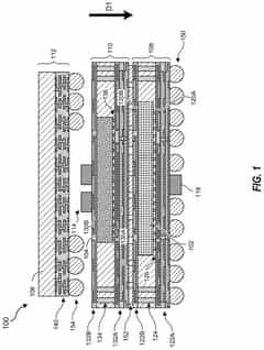
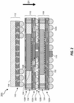
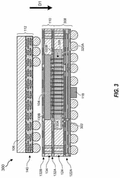
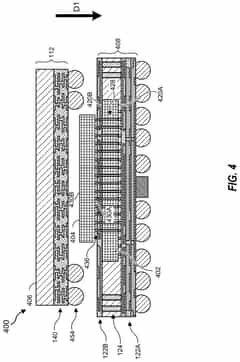
3D chiplet integration using fan-out wafer-level packaging
PatentPendingUS20240274587A1
Innovation
- The use of fan-out wafer-level packaging and three-dimensional packaging techniques for combining semiconductor chips and embedded memory in configurations such as face-to-back, back-to-back, and face-to-face orientations, enabling direct connections between chiplets and reducing assembly package sizes and manufacturing complexity.
Semiconductor chiplet device
PatentActiveUS12230578B2
Innovation
- The semiconductor chiplet device incorporates an interposer layer with at least one decoupling capacitor arranged between the interfaces of the first and second dies, or in the vertical projection area of these interfaces on the package substrate, to form a discharge path that eliminates noise and maintains power integrity.


Interoperability Standards Development
The development of interoperability standards represents a critical milestone in the evolution of chiplet technology. Industry consortia such as Universal Chiplet Interconnect Express (UCIe) have emerged as pivotal forces in establishing common frameworks for chiplet integration. UCIe, founded in 2022 by industry leaders including Intel, AMD, Arm, and TSMC, has rapidly gained momentum as the primary standardization effort for die-to-die interconnects.
These standards focus on three essential layers of interoperability: physical, protocol, and software. The physical layer standards address die-to-die connections, bump patterns, and power delivery specifications. Protocol standards define communication mechanisms between chiplets, including data formats, error handling, and flow control. Software standards ensure operating systems and applications can effectively manage multi-chiplet systems.
Current standardization efforts have achieved significant progress in defining physical interconnects, with UCIe 1.0 establishing specifications for both standard and advanced packaging technologies. The standard supports both parallel and serial interfaces, accommodating different bandwidth and latency requirements across various applications.
Despite these advancements, challenges remain in protocol standardization. Different chiplet types—processors, memory, accelerators—have distinct communication requirements that complicate the development of universal protocols. Industry stakeholders are working to balance flexibility with efficiency, developing modular protocol specifications that can adapt to diverse chiplet combinations.
Security and authentication standards represent another critical development area. As chiplets from multiple vendors are integrated into single packages, mechanisms for secure identification, authentication, and trusted execution become essential. The UCIe consortium has established working groups specifically focused on developing security standards for multi-vendor chiplet ecosystems.
Testing and validation standards are evolving to address the unique challenges of chiplet-based designs. Known-good-die testing methodologies and standardized test interfaces are being developed to ensure reliable integration. These standards aim to reduce integration risks and enable broader adoption of chiplet technology across the semiconductor industry.
The pace of standards development has accelerated significantly, with adoption timelines shortening from years to months. This rapid evolution reflects the industry's recognition that standardization is not merely beneficial but essential for the chiplet ecosystem to flourish and deliver on its promise of enhanced semiconductor performance, cost efficiency, and design flexibility.
Supply Chain Implications for Chiplet Adoption
The adoption of chiplet technology is fundamentally reshaping semiconductor supply chains, creating both opportunities and challenges for industry participants. Traditional monolithic chip production typically involves a linear supply chain with clear boundaries between design houses, foundries, and packaging facilities. In contrast, chiplet architecture necessitates a more complex, interconnected ecosystem where multiple suppliers must collaborate closely to ensure compatibility and performance.
For semiconductor manufacturers, chiplet adoption requires significant adjustments to procurement strategies. Instead of sourcing complete integrated circuits, companies must now coordinate the acquisition of multiple chiplet components from various suppliers, each potentially using different process nodes. This diversification can mitigate supply chain risks by reducing dependence on single suppliers but simultaneously increases coordination complexity and potential points of failure.
The standardization of chiplet interfaces plays a crucial role in supply chain resilience. As industry standards like UCIe (Universal Chiplet Interconnect Express) gain traction, they enable greater interoperability between chiplets from different vendors. This standardization reduces vendor lock-in and allows manufacturers to substitute components more easily when facing supply constraints, effectively creating a more flexible and adaptable supply network.
From a geographical perspective, chiplet technology may accelerate supply chain regionalization. Different regions can specialize in specific types of chiplets based on their technological strengths and manufacturing capabilities. This specialization could lead to more distributed production networks, potentially reducing geopolitical vulnerabilities while creating new interdependencies between regions with complementary capabilities.
Inventory management becomes increasingly sophisticated in a chiplet-based supply chain. Companies must balance the benefits of component commonality against the risks of shortages. The modular nature of chiplets allows for more strategic inventory policies, where critical or long-lead-time components can be stockpiled while others are produced just-in-time.
Testing and quality assurance processes also undergo significant transformation. The need to verify both individual chiplet functionality and system-level integration introduces new supply chain checkpoints. This requires specialized testing equipment and expertise, potentially creating new service opportunities within the semiconductor ecosystem for specialized testing providers.
For smaller industry players, chiplet standardization may lower barriers to entry by enabling them to focus on specific components rather than entire systems. This could foster innovation and competition, ultimately strengthening the overall supply chain through greater diversity of suppliers and solutions.
Unlock deeper insights with PatSnap Eureka Quick Research — get a full tech report to explore trends and direct your research. Try now!
Generate Your Research Report Instantly with AI Agent
Supercharge your innovation with PatSnap Eureka AI Agent Platform!