How Chiplet Integration and Regulation Coexist in Manufacturing
OCT 15, 202510 MIN READ
Generate Your Research Report Instantly with AI Agent
Patsnap Eureka helps you evaluate technical feasibility & market potential.
Chiplet Integration Background and Objectives
The evolution of semiconductor technology has been characterized by continuous miniaturization following Moore's Law for decades. However, as traditional scaling approaches physical limitations, chiplet integration has emerged as a revolutionary paradigm shift in semiconductor manufacturing. This approach involves disaggregating monolithic system-on-chip (SoC) designs into smaller functional blocks called chiplets, which are then integrated using advanced packaging technologies. The concept originated in the early 2010s but gained significant momentum around 2017-2018 when major semiconductor companies began implementing chiplet-based architectures in their high-performance products.
The primary objective of chiplet integration is to overcome the yield, cost, and performance challenges associated with monolithic integration at advanced nodes. By manufacturing different functional components on their optimal process nodes and then integrating them, manufacturers can achieve better yields, reduce costs, and optimize performance. This approach also enables the mixing of heterogeneous technologies (digital, analog, memory) that would be difficult or impossible to integrate monolithically.
The technological trajectory of chiplets has been accelerating, with innovations in die-to-die interconnects, packaging materials, and integration methodologies. From early implementations using organic substrates and traditional flip-chip technologies, the industry has progressed to advanced packaging solutions like EMIB (Embedded Multi-die Interconnect Bridge), CoWoS (Chip-on-Wafer-on-Substrate), and Foveros 3D stacking. These technologies enable higher bandwidth, lower latency, and improved power efficiency in inter-chiplet communications.
Regulatory considerations have evolved alongside technical developments, creating a complex landscape where manufacturing innovation must coexist with standardization efforts, intellectual property frameworks, and quality assurance protocols. The industry faces the challenge of establishing standards for chiplet interfaces and testing methodologies while maintaining the flexibility needed for innovation.
The convergence of chiplet integration and regulatory frameworks aims to establish a sustainable ecosystem where different vendors' chiplets can interoperate seamlessly. This requires not only technical standardization but also regulatory alignment across different jurisdictions, particularly regarding export controls, security requirements, and reliability standards. Organizations like CHIPS Alliance, Open Compute Project, and UCIe (Universal Chiplet Interconnect Express) consortium are working to develop open standards for chiplet interfaces.
Looking forward, the objectives for chiplet integration include achieving true "plug-and-play" interoperability between chiplets from different vendors, reducing integration costs, improving energy efficiency, and establishing comprehensive testing and validation methodologies that satisfy regulatory requirements while accelerating time-to-market.
Market Demand Analysis for Chiplet Technology
The global chiplet market is experiencing unprecedented growth, driven by the increasing demand for advanced computing solutions across various industries. Current market projections indicate that the chiplet technology market will reach approximately $5.8 billion by 2024, with a compound annual growth rate (CAGR) of 40.7% from 2022 to 2027. This remarkable growth trajectory underscores the critical importance of chiplet technology in addressing the limitations of traditional monolithic chip designs.
The primary market drivers for chiplet technology stem from several converging factors. Data centers and cloud service providers are seeking more efficient, high-performance computing solutions to handle exponentially growing workloads. These entities represent the largest market segment, accounting for roughly 38% of current chiplet demand. The artificial intelligence and machine learning sectors follow closely, contributing approximately 27% of market demand, as these applications require increasingly complex computational capabilities that traditional chip designs struggle to deliver.
Consumer electronics manufacturers are also rapidly adopting chiplet technology, particularly in high-end smartphones, tablets, and gaming devices. This segment represents about 19% of the current market share and is expected to grow significantly as chiplet manufacturing becomes more standardized and cost-effective. The automotive industry, particularly for advanced driver-assistance systems and autonomous vehicles, is emerging as another significant market, currently at 8% but projected to reach 15% by 2026.
From a geographical perspective, North America leads the chiplet market with approximately 42% share, followed by Asia-Pacific at 38%, Europe at 16%, and other regions at 4%. However, the Asia-Pacific region is expected to demonstrate the fastest growth rate in the coming years due to increasing investments in semiconductor manufacturing infrastructure, particularly in Taiwan, South Korea, and China.
The market demand is further characterized by specific requirements that highlight the need for regulatory frameworks to coexist with integration technologies. Customers across all segments are demanding improved power efficiency, with benchmarks indicating that chiplet-based designs can reduce power consumption by up to 30% compared to traditional monolithic approaches. Performance scalability remains another critical demand factor, with customers seeking solutions that can be easily upgraded or reconfigured without complete system redesigns.
Interoperability standards represent perhaps the most significant market demand influencing the regulatory landscape. Industry surveys indicate that 78% of potential chiplet technology adopters consider standardized interfaces and protocols essential for their implementation decisions. This demand is driving collaborative efforts across the industry to establish common frameworks that balance innovation with necessary regulatory oversight.
Current Challenges in Chiplet Integration and Regulation
The integration of chiplet technology into semiconductor manufacturing presents significant challenges at the intersection of technical implementation and regulatory compliance. Current manufacturing processes face difficulties in achieving consistent inter-chiplet connections while maintaining high yields. The primary technical hurdle remains the development of reliable and standardized interfaces between chiplets, with manufacturers struggling to balance proprietary designs against the need for industry-wide compatibility.
Manufacturing tolerances present another substantial challenge, as the assembly of multiple chiplets requires unprecedented precision in placement and bonding. Even minor misalignments can result in connection failures or performance degradation, necessitating advanced quality control systems that many facilities have yet to fully implement. These technical challenges are compounded by the lack of unified testing methodologies for multi-chiplet systems, making quality assurance particularly complex.
From a regulatory perspective, chiplet-based designs face a fragmented landscape of standards and certifications. Different regions maintain varying requirements for semiconductor products, creating compliance difficulties for manufacturers targeting global markets. The modular nature of chiplets further complicates regulatory approval, as each component may originate from different suppliers with distinct manufacturing processes and documentation practices.
Intellectual property protection represents another significant regulatory challenge. The collaborative nature of chiplet-based designs often involves multiple companies contributing different components, creating complex IP ownership scenarios. Manufacturers must navigate intricate licensing agreements while protecting their innovations, all within regulatory frameworks that were largely designed for traditional monolithic chip production.
Supply chain security and verification have emerged as critical concerns, particularly as regulatory bodies worldwide increase scrutiny of semiconductor components in sensitive applications. Manufacturers must implement robust traceability systems to document the origin and handling of each chiplet, often across international boundaries and multiple suppliers.
Energy efficiency regulations present additional compliance challenges, as the disaggregated nature of chiplet designs can impact overall power consumption characteristics. Manufacturers must optimize inter-chiplet communication to minimize energy losses while meeting increasingly stringent regulatory requirements for electronic device efficiency in major markets.
The coexistence of these technical and regulatory challenges creates a complex landscape that manufacturers must navigate. Companies leading in chiplet integration are developing comprehensive approaches that address both dimensions simultaneously, recognizing that solutions must satisfy technical performance requirements while maintaining full regulatory compliance across global markets.
Current Regulatory Compliance Solutions for Chiplets
01 Advanced Interconnect Technologies for Chiplet Integration
Various interconnect technologies are being developed to enable efficient chiplet integration. These include advanced packaging methods, through-silicon vias (TSVs), and high-bandwidth interconnects that facilitate communication between different chiplets. These technologies aim to minimize signal delay, reduce power consumption, and enhance overall system performance by optimizing the connections between integrated chiplets.- Interconnect technologies for chiplet integration: Various interconnect technologies are employed to enable efficient communication between chiplets in multi-die packages. These include advanced micro-bump arrays, through-silicon vias (TSVs), and high-bandwidth interposers that facilitate high-speed data transfer between chiplets. These interconnect solutions address challenges related to signal integrity, power delivery, and thermal management while enabling heterogeneous integration of different chiplet technologies.
- Packaging architectures for chiplet integration: Various packaging architectures have been developed to optimize chiplet integration, including 2.5D and 3D stacking approaches. These architectures utilize silicon interposers, organic substrates, or advanced bridge technologies to connect multiple chiplets within a single package. The packaging solutions address thermal challenges, mechanical stress, and electrical performance requirements while enabling higher integration density and improved system performance.
- Design methodologies for chiplet-based systems: Specialized design methodologies have been developed to address the unique challenges of chiplet-based systems. These include partitioning strategies for dividing system functionality across multiple chiplets, interface standardization to ensure compatibility between chiplets from different vendors, and design-for-test approaches that enable efficient testing of integrated chiplet systems. These methodologies help manage complexity and optimize performance in multi-chiplet designs.
- Power and thermal management for chiplet integration: Advanced power and thermal management techniques are essential for chiplet integration, including dynamic power distribution networks, localized cooling solutions, and thermal-aware placement strategies. These approaches help manage heat dissipation across multiple chiplets with different power profiles and ensure reliable operation under varying workloads. Effective power and thermal management enables higher performance while maintaining system reliability in chiplet-based designs.
- Testing and yield optimization for chiplet-based systems: Specialized testing methodologies and yield optimization techniques have been developed for chiplet-based systems. These include known-good-die testing before integration, built-in self-test capabilities for assembled packages, and redundancy schemes that improve manufacturing yield. These approaches address the challenges of testing complex multi-die packages and ensure reliable operation of integrated chiplet systems while reducing overall manufacturing costs.
02 Thermal Management Solutions for Chiplet Architectures
Effective thermal management is crucial for chiplet-based designs due to the high power density and heat generation. Various cooling solutions and thermal interface materials are being developed specifically for chiplet architectures. These include advanced heat spreaders, liquid cooling systems, and thermal interface materials that efficiently dissipate heat from densely packed chiplets, ensuring reliable operation and preventing thermal-induced performance degradation.Expand Specific Solutions03 Heterogeneous Integration of Chiplets
Heterogeneous integration involves combining chiplets manufactured using different process technologies or from different vendors into a single package. This approach allows for optimizing each component for its specific function while maintaining system-level integration. It enables the combination of logic, memory, analog, and RF components manufactured at their optimal process nodes, resulting in improved performance, reduced costs, and enhanced functionality compared to monolithic designs.Expand Specific Solutions04 Design and Testing Methodologies for Chiplet-Based Systems
Specialized design and testing methodologies are being developed to address the unique challenges of chiplet-based systems. These include new EDA tools for chiplet-aware design, pre-silicon validation techniques, and post-assembly testing strategies. These methodologies help ensure proper functionality, signal integrity, and reliability of the integrated chiplets while streamlining the design process and reducing time-to-market for chiplet-based products.Expand Specific Solutions05 Standardization and Interoperability Frameworks for Chiplets
Industry efforts are focused on developing standardized interfaces and protocols to enable interoperability between chiplets from different vendors. These standards define electrical, physical, and logical interfaces that allow chiplets to be mixed and matched in a plug-and-play fashion. Standardization efforts aim to create an ecosystem where chiplets from various suppliers can work together seamlessly, fostering innovation and reducing development costs across the semiconductor industry.Expand Specific Solutions
Key Industry Players in Chiplet Manufacturing
The chiplet integration market is currently in a growth phase, characterized by increasing adoption across semiconductor manufacturing. The global market size is expanding rapidly, driven by demand for advanced computing solutions that overcome traditional monolithic chip limitations. Technologically, the field is maturing with companies like TSMC, Intel, and AMD leading innovation in chiplet architecture and integration techniques. TSMC has established advanced packaging technologies, while Intel's Foveros and EMIB technologies demonstrate significant progress in 3D integration. AMD has successfully commercialized chiplet designs in high-performance processors, and Micron is advancing memory integration solutions. Regulatory frameworks are evolving alongside these technological developments, with companies like GLOBALFOUNDRIES and SMIC navigating complex manufacturing compliance requirements while maintaining innovation momentum.
Taiwan Semiconductor Manufacturing Co., Ltd.
Technical Solution: TSMC has pioneered advanced chiplet integration through their CoWoS (Chip-on-Wafer-on-Substrate) and InFO (Integrated Fan-Out) packaging technologies. Their approach involves sophisticated interposer designs that enable high-bandwidth, low-latency communication between chiplets while maintaining compliance with manufacturing regulations. TSMC's 3DFabric technology platform integrates front-end process technologies with advanced packaging solutions, allowing heterogeneous integration of chiplets manufactured using different process nodes. They've implemented strict quality control systems that satisfy both international manufacturing standards and local regulatory requirements, with their manufacturing facilities certified to ISO standards while maintaining compliance with environmental regulations through their green manufacturing initiatives[1][3]. TSMC has also developed specialized testing protocols for chiplet-based designs that ensure regulatory compliance at each manufacturing stage.
Strengths: Industry-leading advanced packaging technologies with proven high-volume manufacturing capability; comprehensive ecosystem support for chiplet design integration; established regulatory compliance frameworks across global operations. Weaknesses: Higher integration costs compared to monolithic designs; complex supply chain management required for multi-vendor chiplet solutions; thermal management challenges in densely packed chiplet configurations.
Intel Corp.
Technical Solution: Intel has developed their Advanced Interface Bus (AIB) and EMIB (Embedded Multi-die Interconnect Bridge) technologies specifically for chiplet integration. Their Foveros 3D packaging technology enables vertical stacking of chiplets with through-silicon vias (TSVs), allowing for more complex integration while addressing regulatory requirements. Intel's approach includes a comprehensive design validation process that ensures chiplets from different sources can be integrated while maintaining compliance with manufacturing regulations. Their Universal Chiplet Interconnect Express (UCIe) standard, which they've opened to the industry, establishes protocols for chiplet interoperability while incorporating regulatory considerations into the specification[2]. Intel has implemented a "design for regulation" methodology where regulatory requirements are considered early in the chiplet design process, including electromagnetic interference (EMI) mitigation, thermal management, and materials compliance. Their manufacturing facilities incorporate automated compliance verification systems that track regulatory adherence throughout the production process.
Strengths: Comprehensive vertical integration from design to manufacturing; established standards leadership with UCIe; extensive experience navigating global regulatory environments for semiconductor products. Weaknesses: Historical challenges in transitioning to advanced process nodes; complex internal bureaucracy can slow regulatory adaptation; higher manufacturing costs compared to some competitors.
Core Patents and Technical Literature in Chiplet Integration
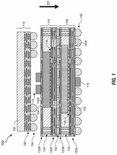
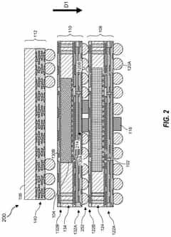
3D chiplet integration using fan-out wafer-level packaging
PatentPendingUS20240274587A1
Innovation
- The use of fan-out wafer-level packaging and three-dimensional packaging techniques for combining semiconductor chips and embedded memory in configurations such as face-to-back, back-to-back, and face-to-face orientations, enabling direct connections between chiplets and reducing assembly package sizes and manufacturing complexity.
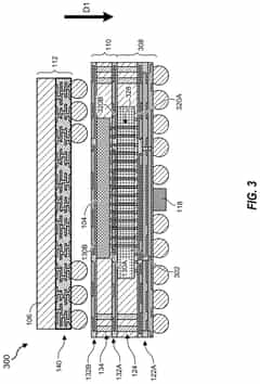
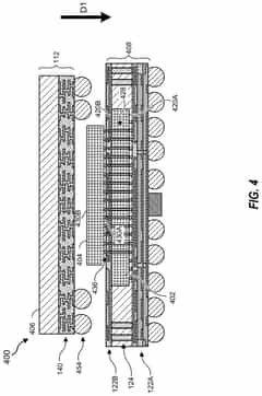
Composite IC chips including a chiplet embedded within metallization layers of a host IC chip
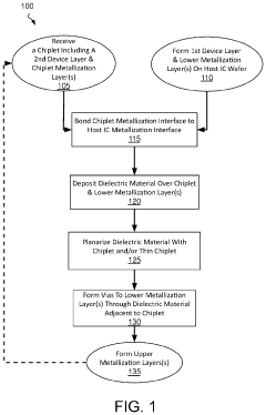
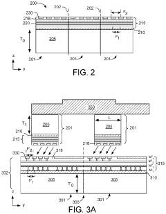
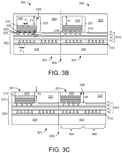
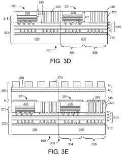
PatentActiveUS20210375830A1
Innovation
- The integration of an IC chiplet within the back-end metallization layers of a host IC chip using hybrid monolithic and die-level bonding techniques, allowing for higher density interconnections and flexible alignment, which enhances interconnect density and supports fine pitches.
Global Regulatory Framework for Semiconductor Manufacturing
The global regulatory landscape for semiconductor manufacturing has evolved significantly to address the unique challenges posed by chiplet integration technologies. Different regions have established varying approaches to regulate this emerging field, creating a complex framework that manufacturers must navigate. In the United States, the CHIPS Act has allocated substantial funding for domestic semiconductor production while simultaneously implementing export controls on advanced chip technologies to China, directly impacting chiplet manufacturing strategies.
The European Union has developed the European Chips Act, focusing on strengthening the semiconductor supply chain resilience while establishing specific regulatory provisions for chiplet integration. These regulations emphasize standardization of interfaces between chiplets to ensure interoperability across the European market, creating both challenges and opportunities for manufacturers implementing multi-chiplet designs.
In Asia, regulatory approaches differ significantly between countries. Japan and South Korea have implemented policies that encourage chiplet innovation through targeted incentives while maintaining strict quality control standards. China's regulatory framework focuses on achieving semiconductor self-sufficiency, with particular emphasis on chiplet technology as a pathway to overcome certain technology access limitations.
International standards organizations play a crucial role in harmonizing these diverse regulatory frameworks. The IEEE, JEDEC, and SEMI have established working groups specifically focused on chiplet integration standards, creating technical specifications that help manufacturers comply with various regional regulations simultaneously. These standards address critical aspects including thermal management, power delivery, and signal integrity across chiplet interfaces.
Compliance challenges remain significant for global manufacturers implementing chiplet designs. The heterogeneous nature of chiplets, often manufactured in different facilities or even different countries, creates complex regulatory scenarios regarding country of origin determinations, export controls, and intellectual property protection. Companies must implement sophisticated tracking systems to document the regulatory compliance of each chiplet component throughout the manufacturing process.
Environmental regulations increasingly impact chiplet manufacturing, with different regions imposing varying requirements for chemical usage, waste management, and energy efficiency. The modular nature of chiplet designs offers potential advantages in meeting sustainability goals through more efficient resource utilization and extended product lifecycles, though manufacturers must navigate different regional interpretations of environmental standards.
Looking forward, regulatory harmonization efforts are emerging through multilateral agreements and industry consortia focused specifically on chiplet technologies. These initiatives aim to reduce compliance burdens while maintaining necessary oversight of this strategically important technology domain.
Supply Chain Security Considerations for Chiplet Technology
The security of supply chains has become a critical concern in chiplet technology implementation, particularly as manufacturing processes become increasingly distributed across multiple vendors and geographies. Chiplet integration introduces unique vulnerabilities due to the disaggregation of traditionally monolithic chip designs into smaller functional blocks sourced from various suppliers.
The multi-vendor nature of chiplet ecosystems creates numerous entry points for potential security breaches. Each chiplet may originate from different fabrication facilities with varying security protocols and standards, increasing the risk of compromised components entering the supply chain. This distributed manufacturing model necessitates comprehensive tracking mechanisms to ensure authenticity and integrity throughout the production lifecycle.
Hardware trojans represent a significant threat in chiplet-based systems. These malicious modifications can be inserted during design or manufacturing phases, potentially remaining dormant until triggered under specific conditions. The modular nature of chiplets complicates detection efforts, as security testing must account for interactions between independently manufactured components that may not exhibit vulnerabilities when tested in isolation.
Regulatory frameworks worldwide are evolving to address these emerging security challenges. The CHIPS Act in the United States and similar initiatives in Europe and Asia aim to strengthen domestic semiconductor manufacturing capabilities while establishing security standards for chiplet integration. These regulations increasingly mandate supply chain transparency, requiring manufacturers to implement robust traceability systems and security certifications.
Secure integration protocols are being developed specifically for chiplet technologies. These include cryptographic authentication mechanisms that verify the legitimacy of each chiplet before integration, preventing counterfeit components from entering the assembly process. Zero-trust architectures are becoming essential, where each chiplet must continuously prove its authenticity rather than being trusted by default once integrated.
Physical security measures at manufacturing facilities must be complemented by digital safeguards throughout the supply chain. This includes secure data exchange protocols between design houses and foundries, encrypted design files, and tamper-evident packaging for chiplet transport. The implementation of blockchain-based tracking systems offers promising solutions for maintaining immutable records of chiplet provenance.
Industry consortia like the Universal Chiplet Interconnect Express (UCIe) are working to establish security standards specifically for chiplet ecosystems. These collaborative efforts aim to create common security frameworks that can be adopted across the industry, ensuring interoperability while maintaining robust protection against supply chain attacks.
Unlock deeper insights with Patsnap Eureka Quick Research — get a full tech report to explore trends and direct your research. Try now!
Generate Your Research Report Instantly with AI Agent
Supercharge your innovation with Patsnap Eureka AI Agent Platform!