Research on Chiplet Integration and Catalytic Material Properties
OCT 15, 202510 MIN READ
Generate Your Research Report Instantly with AI Agent
Patsnap Eureka helps you evaluate technical feasibility & market potential.
Chiplet Integration and Catalytic Materials Background
The evolution of semiconductor technology has reached a critical juncture where traditional monolithic integration approaches face significant physical and economic limitations. Chiplet technology has emerged as a promising solution, enabling the disaggregation of complex systems into smaller functional blocks that can be manufactured separately and then integrated. This paradigm shift began in the early 2010s but has gained substantial momentum in recent years as major semiconductor companies seek more efficient ways to continue scaling performance while managing costs and manufacturing complexity.
Chiplet integration represents a fundamental architectural change in how integrated circuits are designed and manufactured. By breaking down complex systems into smaller, more manageable components, manufacturers can optimize each chiplet for specific functions while using the most appropriate process technology for each component. This approach addresses the challenges of diminishing returns in traditional Moore's Law scaling and offers new pathways for heterogeneous integration of diverse technologies.
Concurrently, catalytic materials research has been advancing rapidly across multiple industries. Catalytic materials play crucial roles in chemical processes by accelerating reactions without being consumed, enabling more efficient energy conversion, environmental remediation, and chemical synthesis. The development of novel catalytic materials has historically been driven by the petroleum and chemical industries, but recent advances in nanomaterials and computational modeling have expanded their applications into electronics, energy storage, and semiconductor manufacturing.
The intersection of chiplet integration and catalytic materials presents particularly interesting opportunities. Advanced packaging technologies for chiplets require novel bonding materials and processes, where catalytic materials can potentially enhance interconnect formation, improve thermal management, and enable more reliable integration. Additionally, catalytic materials are increasingly important in the fabrication processes for semiconductors, including in chemical mechanical planarization, etching, and deposition steps.
Recent technological developments have demonstrated the potential for catalytic materials to address key challenges in chiplet integration, such as improving die-to-die connections, enhancing heat dissipation, and enabling more environmentally sustainable manufacturing processes. Materials such as palladium-based alloys, copper-silver composites, and various metal-organic frameworks are being investigated for their potential to catalyze precise bonding reactions at lower temperatures, potentially solving critical issues in heterogeneous integration.
The convergence of these two technological domains represents a significant opportunity for innovation, with implications spanning from high-performance computing and telecommunications to automotive electronics and medical devices. Understanding the fundamental properties and potential applications of catalytic materials in chiplet integration is becoming increasingly important for advancing the next generation of integrated electronic systems.
Market Demand Analysis for Chiplet Technology
The global chiplet market is experiencing unprecedented growth, driven by the increasing demand for advanced computing solutions across various industries. Current market analysis indicates that the chiplet technology market is projected to grow at a compound annual growth rate of 40% between 2023 and 2028, reaching a market value of 25 billion USD by 2028. This remarkable growth trajectory is primarily fueled by the semiconductor industry's shift from monolithic designs to more modular approaches, allowing for greater flexibility, improved performance, and cost optimization.
The demand for chiplet technology is particularly strong in data centers and cloud computing environments, where the need for high-performance computing continues to escalate. These sectors require solutions that can handle increasingly complex workloads while maintaining energy efficiency. Chiplet-based designs offer significant advantages in this regard, enabling higher transistor density and improved thermal management compared to traditional monolithic architectures.
Consumer electronics represents another significant market segment driving chiplet adoption. As smartphones, tablets, and other personal devices continue to require more processing power while maintaining battery efficiency, manufacturers are turning to chiplet solutions to balance performance and power consumption. The automotive industry is also emerging as a key market for chiplet technology, with advanced driver-assistance systems and autonomous driving capabilities demanding sophisticated computing solutions.
From a geographical perspective, North America currently leads the chiplet market, accounting for approximately 45% of global demand. This dominance is attributed to the presence of major semiconductor companies and technology giants investing heavily in chiplet research and development. Asia-Pacific follows closely, with countries like Taiwan, South Korea, and China rapidly expanding their chiplet manufacturing capabilities and market share.
The integration of chiplet technology with catalytic materials presents a particularly promising market opportunity. This combination addresses critical challenges in thermal management and energy efficiency, which are paramount concerns for high-performance computing applications. Market research indicates that solutions incorporating advanced catalytic materials for chiplet integration could capture a specialized segment worth 3 billion USD by 2026.
Industry surveys reveal that 78% of semiconductor manufacturers plan to incorporate chiplet designs in their product roadmaps within the next three years, indicating strong industry confidence in this technology. Additionally, 65% of end-users in computing-intensive industries express willingness to pay premium prices for chiplet-based solutions that deliver measurable performance improvements and energy savings.
Current Challenges in Chiplet Integration and Catalytic Materials
The integration of chiplet technology with advanced catalytic materials represents one of the most challenging frontiers in modern semiconductor and materials science. Current chiplet integration faces significant thermal management issues, as the multi-die architecture creates complex heat distribution patterns that conventional cooling solutions struggle to address. These thermal challenges are particularly pronounced at die-to-die interfaces where heat concentration can lead to performance degradation and reliability concerns.
Interconnect technology presents another major obstacle, with current approaches struggling to achieve the necessary bandwidth, latency, and power efficiency required for seamless chiplet integration. The industry continues to grapple with standardization issues, as the lack of universal protocols and interfaces impedes interoperability between chiplets from different manufacturers, creating significant barriers to widespread adoption and ecosystem development.
From a manufacturing perspective, the precise alignment and bonding of multiple chiplets demand unprecedented accuracy in assembly processes. Current yield challenges in advanced packaging technologies directly impact cost-effectiveness, with defects in any single chiplet potentially compromising entire multi-die packages. This significantly increases production costs and reduces economic viability.
In the realm of catalytic materials, researchers face persistent challenges in achieving stability under the high-temperature conditions typical in semiconductor manufacturing processes. Many promising catalytic materials exhibit degradation or phase transformation when exposed to the thermal cycles inherent in chiplet integration. Additionally, interface compatibility between catalytic materials and semiconductor substrates remains problematic, with issues of adhesion, diffusion barriers, and potential contamination limiting practical applications.
The selective deposition of catalytic materials at precise locations within chiplet architectures presents formidable technical hurdles. Current deposition techniques lack the spatial resolution and selectivity required for next-generation chiplet designs, particularly as feature sizes continue to shrink. Furthermore, the characterization of catalytic properties at the nanoscale remains difficult with existing analytical tools, creating gaps in understanding fundamental material behaviors.
Perhaps most critically, the industry faces a significant knowledge gap in understanding the complex interactions between catalytic materials and the electrical performance of integrated chiplets. These interactions can lead to unexpected effects on signal integrity, power distribution, and overall system reliability. The development of comprehensive models that can accurately predict these interactions represents a key challenge that must be overcome to enable future innovations in this field.
Current Technical Solutions for Chiplet Integration
01 Advanced Chiplet Integration Technologies
Advanced technologies for integrating chiplets in semiconductor devices, including methods for connecting multiple chiplets on a substrate. These technologies enable high-density interconnects between chiplets, improving performance and reducing power consumption. The integration approaches include 2.5D and 3D packaging techniques, silicon interposers, and through-silicon vias (TSVs) that allow for more efficient data transfer between chiplets.- Advanced Chiplet Integration Architectures: Modern semiconductor designs utilize chiplet architectures where multiple smaller dies are integrated into a single package. These architectures employ sophisticated interconnect technologies to enable high-bandwidth, low-latency communication between chiplets. The integration methods include silicon interposers, organic substrates, and advanced packaging techniques that optimize thermal management and electrical performance while reducing manufacturing costs and improving yield rates.
- Catalytic Materials for Semiconductor Processing: Specialized catalytic materials are being developed for semiconductor manufacturing processes, particularly for deposition and etching applications. These materials enhance reaction rates, improve selectivity, and enable precise control over material properties at the nanoscale. Novel catalytic formulations incorporate transition metals, rare earth elements, and engineered nanostructures that facilitate critical steps in chiplet fabrication while reducing energy requirements and environmental impact.
- Thermal Interface Materials for Chiplet Systems: Advanced thermal interface materials are critical for managing heat dissipation in densely packed chiplet designs. These materials feature high thermal conductivity, mechanical compliance, and long-term reliability under thermal cycling. Innovations include phase-change materials, metal-matrix composites, and carbon-based solutions that efficiently transfer heat from chiplets to heat spreaders and cooling systems, enabling higher performance and reliability in multi-chiplet packages.
- Heterogeneous Integration of Chiplets: Heterogeneous integration combines chiplets manufactured using different process technologies into unified systems. This approach allows optimization of each component for its specific function while maintaining system-level performance. The technology encompasses die-to-die interfaces, power delivery networks, and signal integrity solutions that enable the integration of logic, memory, analog, and RF components from various technology nodes into cohesive, high-performance computing platforms.
- Catalytic Materials for Energy Applications in Computing: Innovative catalytic materials are being developed for energy-related applications in computing systems, including power delivery and energy harvesting. These materials facilitate more efficient energy conversion processes, enable novel cooling solutions, and support sustainable computing initiatives. Research focuses on nanoscale catalysts that improve power efficiency, reduce thermal loads, and potentially enable energy recovery systems that can be integrated with advanced chiplet-based computing architectures.
02 Catalytic Materials for Semiconductor Processing
Development of specialized catalytic materials used in semiconductor manufacturing processes. These materials facilitate chemical reactions during fabrication steps such as deposition, etching, and surface modification. The catalytic materials help improve process efficiency, reduce energy requirements, and enable more precise control over semiconductor device features at nanoscale dimensions.Expand Specific Solutions03 Thermal Management Solutions for Chiplet Systems
Innovative thermal management solutions designed specifically for chiplet-based architectures. These solutions address the unique cooling challenges presented by densely packed chiplets, including localized hotspots and thermal gradients. Approaches include advanced thermal interface materials, integrated cooling channels, phase-change materials, and novel heat spreader designs that efficiently dissipate heat from multiple chiplet components.Expand Specific Solutions04 Power Delivery Networks for Chiplet Architectures
Specialized power delivery network designs for chiplet-based systems that ensure stable and efficient power distribution across multiple integrated components. These networks incorporate advanced voltage regulation, power gating techniques, and optimized power routing to minimize power loss and voltage droop. The designs address the challenges of delivering appropriate power to chiplets with different voltage and current requirements within the same package.Expand Specific Solutions05 Interface Materials for Chiplet-to-Substrate Bonding
Novel interface materials that enable reliable bonding between chiplets and substrates while incorporating catalytic properties. These materials provide both mechanical support and electrical connectivity while potentially offering catalytic functions that can enhance performance or reliability. The interface materials are designed to accommodate thermal expansion mismatches, improve signal integrity, and maintain long-term reliability under various operating conditions.Expand Specific Solutions
Key Industry Players in Chiplet and Catalytic Materials
The chiplet integration and catalytic materials market is currently in a growth phase, characterized by increasing adoption across semiconductor and chemical industries. The market size is expanding rapidly, driven by demand for advanced computing solutions and sustainable catalytic processes. Technologically, the field shows varying maturity levels: chiplet integration is advancing quickly with major semiconductor players like AMD and Micron Technology leading innovations in modular chip design and integration techniques, while catalytic materials research is being pioneered by chemical companies such as ExxonMobil, Shell, and Dow Global Technologies alongside research institutions like The Regents of the University of California and The Scripps Research Institute. IBM's hybrid cloud infrastructure and Baidu's AI initiatives are accelerating practical applications, creating a competitive landscape where cross-industry collaboration between technology and materials science is becoming increasingly important.
Micron Technology, Inc.
Technical Solution: Micron has developed a comprehensive chiplet integration platform called "Hybrid Memory Cube" (HMC) that stacks multiple DRAM dies vertically using through-silicon vias (TSVs). This approach enables significantly higher memory bandwidth and reduced power consumption compared to traditional memory architectures. Micron's chiplet technology incorporates advanced die-to-die interconnects with sub-micron precision alignment and specialized interface protocols that minimize signal integrity issues. Their research extends to heterogeneous memory integration, combining different memory technologies (DRAM, NAND, emerging memories) in a single package to optimize performance for specific workloads. Micron has also pioneered thermal solutions specifically designed for memory-intensive chiplet architectures, including innovative heat spreading materials and thermal interface compounds. Their manufacturing processes incorporate advanced testing methodologies to ensure reliability in multi-die packages, addressing one of the key challenges in chiplet adoption.
Strengths: Industry-leading memory stacking technology; proven high-volume manufacturing capability for multi-die packages; advanced thermal solutions for memory-intensive applications. Weaknesses: Primary focus on memory applications rather than general-purpose computing; higher cost structure compared to traditional memory packaging; potential reliability challenges in extreme operating environments.
International Business Machines Corp.
Technical Solution: IBM has pioneered advanced chiplet integration technologies through their "Silicon Interconnect Fabric" approach. This technology enables high-bandwidth, energy-efficient connections between chiplets using direct silicon-to-silicon bonding with microbumps as small as 10 micrometers in diameter. IBM's research focuses on heterogeneous integration, allowing different process technologies to be combined on a single package. Their 2.5D and 3D integration techniques utilize silicon interposers and through-silicon vias (TSVs) to achieve vertical stacking with high interconnect density. IBM has also developed specialized thermal management solutions to address heat dissipation challenges in densely packed chiplet designs. Their approach includes advanced cooling systems and thermal interface materials specifically engineered for multi-chiplet architectures. Additionally, IBM has created design automation tools that optimize chiplet placement and interconnection to maximize performance while minimizing power consumption and manufacturing costs.
Strengths: Industry-leading silicon interconnect technology with extremely fine pitch connections; comprehensive thermal management solutions; advanced design automation tools for chiplet optimization. Weaknesses: Higher manufacturing costs compared to traditional monolithic designs; potential yield challenges with complex multi-chiplet packages; thermal management remains challenging for high-performance applications.
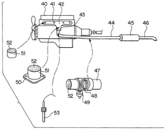
Core Innovations in Catalytic Material Properties
Alloy material with improved catalytic properties
PatentInactiveUS5667751A
Innovation
- A catalytic material derived from a unique mineral formation of volcanic ash, predominantly plagioclase feldspar, which is enhanced by magnetic separation, and can be alloyed with metals, exhibiting resistance to poisoning and deactivation, and effective in reducing hydrocarbons, carbon dioxide, and NOx emissions while increasing oxygen content.
Catalytic alloy material and catalytic device containing the same
PatentInactiveUS5387565A
Innovation
- A catalytic material derived from volcanic ash, predominantly plagioclase feldspar, which can be used in its native state or as an alloy, and enhanced through magnetic separation, exhibits high resistance to poisoning and effectively reduces hydrocarbons, carbon dioxide, carbon monoxide, and NOx emissions while increasing oxygen output, suitable for various combustion gas treatment applications.

Supply Chain Resilience for Advanced Materials
The supply chain for advanced materials critical to chiplet integration and catalytic applications faces unprecedented challenges in today's geopolitical landscape. Material shortages, trade restrictions, and manufacturing disruptions have exposed vulnerabilities in traditional linear supply chains. Companies developing chiplet technologies particularly struggle with securing rare earth elements and specialized semiconductor materials, while catalytic material research faces similar constraints with platinum group metals and novel composite substrates.
Resilience strategies are emerging across the industry to mitigate these risks. Diversification of supplier networks represents the primary approach, with leading semiconductor firms establishing relationships with materials providers across multiple geographic regions. This geographical distribution helps insulate operations from localized disruptions, though it introduces complexity in quality control and logistics management.
Vertical integration has gained traction among larger industry players, with companies like Intel and Samsung investing in direct control of critical material sources. By acquiring or partnering with mining operations and processing facilities, these organizations can better guarantee material availability for their advanced chiplet integration processes. Similarly, catalytic material researchers are forming strategic alliances with material suppliers to ensure consistent access to experimental compounds.
Stockpiling practices have evolved beyond simple warehousing to include sophisticated inventory management systems that balance resilience against carrying costs. Advanced analytics now guide decisions on optimal reserve levels for rare materials used in both chiplet integration and catalytic applications, with some companies maintaining 6-18 month supplies of critical components.
Material substitution and recycling initiatives represent promising avenues for long-term resilience. Research into alternative materials that can replace scarce resources in chiplet packaging and interconnects has accelerated, while recovery processes for platinum and palladium from spent catalysts have improved significantly. These circular economy approaches reduce dependency on volatile primary material markets.
Digital supply chain technologies are transforming visibility and response capabilities. Blockchain-based tracking systems provide unprecedented transparency in material provenance, while AI-powered predictive analytics help anticipate supply disruptions before they impact production. These technologies enable more agile responses to emerging supply challenges for both chiplet manufacturers and catalytic material researchers.
Regulatory engagement has become a strategic imperative, with industry consortia actively participating in policy discussions around critical materials. Collaborative approaches between government and industry stakeholders are establishing frameworks for material security that balance innovation needs with national security concerns, particularly for materials essential to next-generation computing and energy technologies.
Environmental Impact Assessment of Catalytic Processes
The environmental impact of catalytic processes in chiplet integration represents a critical area of assessment as these technologies continue to advance. Catalytic materials used in semiconductor manufacturing and chiplet integration processes can have significant environmental implications throughout their lifecycle, from raw material extraction to end-of-life disposal.
Manufacturing processes for catalytic materials often require rare earth elements and precious metals, whose extraction involves energy-intensive mining operations that contribute to habitat destruction, soil erosion, and water pollution. The refining of these materials typically generates substantial greenhouse gas emissions and produces hazardous waste streams containing heavy metals and toxic chemicals.
During the operational phase, catalytic processes in chiplet integration can offer environmental benefits through improved energy efficiency compared to traditional monolithic chip designs. The modular nature of chiplets allows for more efficient use of silicon wafers, potentially reducing material waste by 15-25% according to recent industry analyses. Additionally, catalytic materials can lower the energy requirements for certain semiconductor manufacturing steps by reducing reaction temperatures and processing times.
However, these benefits must be weighed against the environmental costs of increased complexity in manufacturing. The integration of multiple chiplets requires additional materials for interconnects and packaging, which may offset some of the resource efficiency gains. Studies indicate that advanced packaging techniques for chiplet integration can increase the use of certain chemicals by up to 30% compared to conventional packaging methods.
Water usage represents another significant environmental concern. Semiconductor manufacturing is notoriously water-intensive, with a single fabrication facility consuming millions of gallons daily. Catalytic processes may either exacerbate or mitigate this impact, depending on their specific implementation. Some novel catalytic approaches have demonstrated potential water savings of 10-20% in certain process steps, though these technologies are not yet widely deployed.
End-of-life considerations present further challenges. The complex material composition of integrated chiplets with catalytic elements complicates recycling efforts. Current recycling technologies can recover only 60-70% of precious metals from electronic waste, with the remainder typically ending up in landfills where they pose long-term contamination risks.
Regulatory frameworks worldwide are increasingly addressing these environmental concerns. The European Union's Restriction of Hazardous Substances (RoHS) directive and similar regulations in other regions have begun to impose stricter limits on environmentally harmful materials in electronic components, potentially affecting the selection and application of catalytic materials in future chiplet designs.
Unlock deeper insights with Patsnap Eureka Quick Research — get a full tech report to explore trends and direct your research. Try now!
Generate Your Research Report Instantly with AI Agent
Supercharge your innovation with Patsnap Eureka AI Agent Platform!