

Research on Chiplet Integration in Semiconductor Manufacturing
OCT 15, 20259 MIN READ
Generate Your Research Report Instantly with AI Agent
PatSnap Eureka helps you evaluate technical feasibility & market potential.
Chiplet Technology Evolution and Objectives
The semiconductor industry has witnessed a paradigm shift in recent years, moving from traditional monolithic system-on-chip (SoC) designs toward a more modular approach known as chiplet technology. This evolution began in the early 2010s when semiconductor manufacturers faced increasing challenges with Moore's Law, which had guided industry progress for decades. As process nodes shrank below 10nm, manufacturing costs and complexity increased exponentially, while yield rates declined, creating economic and technical barriers to further integration.
Chiplet technology emerged as a strategic response to these challenges, offering a new integration paradigm where complex systems are built by connecting multiple smaller dies (chiplets) rather than manufacturing a single large die. This approach first gained significant industry attention around 2016-2017 when AMD introduced its Infinity Fabric interconnect technology in Ryzen processors, demonstrating the commercial viability of chiplet-based designs.
The evolution of chiplet technology has been characterized by three distinct phases. The initial phase (2015-2018) focused on basic integration techniques and proof-of-concept designs. The second phase (2019-2021) saw the development of standardized interfaces and more sophisticated packaging technologies. The current phase (2022-present) is marked by industry-wide adoption and the emergence of ecosystem-level standardization efforts such as the Universal Chiplet Interconnect Express (UCIe) consortium.
The primary objectives of chiplet technology research center around overcoming the limitations of traditional monolithic designs. These include improving manufacturing yields by dividing complex systems into smaller, more manageable components; enabling heterogeneous integration of different process technologies within a single package; and reducing development costs by promoting IP reuse and modular design approaches.
From a technical perspective, chiplet integration aims to achieve near-monolithic performance while maintaining the economic advantages of modular design. This requires innovations in die-to-die interconnects, advanced packaging technologies, and thermal management solutions. The industry targets interconnect bandwidths exceeding 2 TB/s with energy efficiency below 1 pJ/bit, while maintaining signal integrity across increasingly complex multi-die packages.
Looking forward, chiplet technology is expected to enable new computing architectures that were previously impractical with monolithic designs. The ultimate goal is to create a "chiplet marketplace" where standardized components from different vendors can be seamlessly integrated, similar to how printed circuit boards revolutionized electronic system design decades ago. This vision requires continued evolution of standards, design tools, and manufacturing processes to support the growing complexity of chiplet-based systems.
Market Demand Analysis for Chiplet Solutions
The global semiconductor market is witnessing a paradigm shift towards chiplet-based architectures, driven by the increasing demand for higher performance, improved power efficiency, and cost-effective scaling solutions. As traditional monolithic chip designs approach physical and economic limits under Moore's Law, chiplet technology has emerged as a promising alternative that allows for the disaggregation of system-on-chip (SoC) designs into smaller, specialized dies that can be manufactured using optimal process nodes and later integrated into a single package.
Market research indicates that the chiplet market is projected to grow at a compound annual growth rate of over 40% from 2023 to 2030, with the total addressable market expected to reach tens of billions of dollars by mid-decade. This explosive growth is primarily fueled by data centers and high-performance computing applications, where the need for specialized accelerators and heterogeneous integration has become critical for handling AI workloads and complex computational tasks.
Cloud service providers and hyperscalers represent the largest current market segment for chiplet solutions, as they continuously seek to optimize performance per watt and total cost of ownership for their massive infrastructure investments. These companies are increasingly adopting chiplet-based designs to achieve customization while maintaining economies of scale.
The consumer electronics sector is also showing growing interest in chiplet technology, particularly for premium smartphones, tablets, and laptops where space constraints and thermal management challenges make heterogeneous integration particularly valuable. Industry analysts predict that by 2025, a significant percentage of high-end consumer devices will incorporate some form of chiplet architecture.
Automotive and industrial applications represent emerging markets with substantial growth potential for chiplet solutions. Advanced driver-assistance systems (ADAS) and autonomous driving platforms require high-performance, energy-efficient computing solutions that can be achieved through chiplet integration. Similarly, industrial automation and edge computing applications benefit from the flexibility and scalability offered by chiplet architectures.
From a regional perspective, North America currently leads in chiplet adoption, followed by East Asia and Europe. However, significant investments in semiconductor manufacturing capabilities across these regions suggest a more distributed market in the coming years, with government initiatives like the CHIPS Act in the United States and similar programs in Europe and Asia accelerating development.
The market demand for chiplet solutions is further strengthened by industry-wide efforts to establish standards for chiplet interfaces and integration methodologies. Initiatives like the Universal Chiplet Interconnect Express (UCIe) consortium are working to create an open ecosystem that would lower barriers to entry and expand the market for chiplet-based designs across multiple vendors and applications.
Current Chiplet Integration Challenges
Despite the promising advancements in chiplet technology, several significant technical challenges currently impede the widespread adoption and optimization of chiplet integration in semiconductor manufacturing. The most pressing challenge remains the development of high-density, high-bandwidth interconnects between chiplets. Current micro-bump technologies face limitations in pitch density, with typical dimensions ranging from 40-55μm, which constrains the number of possible connections between chiplets and ultimately limits system performance.
The heterogeneous integration of chiplets manufactured using different process nodes presents substantial thermal management difficulties. When combining chiplets with varying thermal characteristics and power densities, hotspots can form at interfaces, leading to reliability issues and performance degradation. Current thermal interface materials and heat dissipation solutions struggle to address these complex thermal profiles effectively.
Known-Good-Die (KGD) testing represents another major hurdle in chiplet manufacturing. Unlike traditional monolithic chips that can be tested after packaging, chiplets must be thoroughly tested before integration to ensure system-level functionality. The industry lacks standardized, cost-effective testing methodologies for bare dies, resulting in yield challenges that impact overall economics.
Design and verification complexity increases exponentially in chiplet-based systems. Engineers must account for signal integrity across die boundaries, power delivery network optimization, and clock domain synchronization between multiple chiplets. Current EDA tools are not fully optimized for multi-chiplet design flows, creating bottlenecks in the development process.
Manufacturing alignment precision presents significant challenges, particularly as interconnect densities increase. Current pick-and-place equipment typically achieves alignment accuracy of 1-2μm, which becomes insufficient for advanced chiplet integration requiring sub-micron precision. This limitation affects both yield and performance of chiplet-based systems.
The lack of industry-wide standards for chiplet interfaces represents a fundamental obstacle to ecosystem development. While initiatives like UCIe (Universal Chiplet Interconnect Express) are emerging, fragmentation persists across the industry, hindering interoperability between chiplets from different vendors and limiting the potential for a truly open chiplet marketplace.
Supply chain complexity increases substantially with chiplet-based designs. Managing multiple die sources, ensuring compatibility, and coordinating manufacturing schedules across different facilities introduces logistical challenges that can impact time-to-market and overall product costs. Current supply chain management systems require significant adaptation to handle these multi-sourced manufacturing flows effectively.
Current Chiplet Integration Methodologies
01 Chiplet architecture and integration
Chiplet architecture involves integrating multiple smaller dies (chiplets) into a single package to improve performance, reduce costs, and enhance scalability. This approach allows for mixing and matching different functional blocks manufactured using optimal process technologies. The integration techniques include advanced packaging methods such as 2.5D and 3D integration, interposer technologies, and through-silicon vias (TSVs) to connect the chiplets efficiently.- Chiplet architecture and integration: Chiplet architecture involves integrating multiple smaller dies (chiplets) into a single package to improve performance, reduce costs, and enhance scalability. This modular approach allows for mixing different process technologies and functional blocks. The integration techniques include advanced packaging methods such as 2.5D and 3D integration, interposer technologies, and through-silicon vias (TSVs) to connect chiplets efficiently while maintaining high bandwidth and low latency communication between components.
- Chiplet interconnect technologies: Interconnect technologies are crucial for chiplet-based designs, enabling high-speed communication between different chiplets within a package. These technologies include advanced interfaces, die-to-die connections, and specialized protocols designed to maintain signal integrity across chiplet boundaries. Innovations in this area focus on reducing power consumption while increasing data transfer rates, minimizing latency, and ensuring reliable connections between heterogeneous chiplets manufactured using different process technologies.
- Thermal management for chiplet designs: Thermal management is a critical aspect of chiplet-based systems due to the high power density and potential hotspots created by stacking multiple dies. Solutions include advanced cooling techniques, thermal interface materials, and heat spreading technologies specifically designed for chiplet architectures. These approaches help maintain optimal operating temperatures across all chiplets, prevent thermal throttling, and ensure reliable long-term operation of the integrated system.
- Chiplet-based memory systems: Memory integration in chiplet designs involves specialized approaches to incorporate memory components either as separate chiplets or integrated within processing chiplets. These systems leverage high-bandwidth memory interfaces, memory stacking technologies, and novel cache hierarchies to optimize data access patterns. The chiplet approach allows for flexible memory configurations, enabling systems to be tailored for specific workloads while maintaining high performance and energy efficiency.
- Testing and yield improvement for chiplet technology: Testing methodologies for chiplet-based designs address the unique challenges of verifying functionality across multiple dies before and after integration. These approaches include pre-integration testing of individual chiplets, post-integration system-level testing, and specialized test interfaces between chiplets. By enabling selective use of known-good-dies and facilitating defect isolation, chiplet technology improves overall manufacturing yield compared to monolithic designs, particularly for advanced process nodes where yield challenges are significant.
02 Chiplet interconnect technologies
Interconnect technologies are crucial for chiplet-based designs, enabling high-bandwidth, low-latency communication between different chiplets. These technologies include advanced die-to-die interfaces, silicon bridges, and specialized protocols designed specifically for chiplet communication. The interconnect solutions address challenges related to signal integrity, power delivery, and thermal management while maintaining high performance across the chiplet boundaries.Expand Specific Solutions03 Thermal management in chiplet designs
Thermal management is a critical aspect of chiplet-based systems due to the high power density and potential hotspots at chiplet interfaces. Solutions include specialized cooling structures, thermal interface materials optimized for chiplet packages, and dynamic thermal management techniques that monitor and regulate temperature across multiple chiplets. These approaches ensure reliable operation and consistent performance across the entire chiplet-based system.Expand Specific Solutions04 Chiplet-based memory and processing architectures
Chiplet technology enables novel memory and processing architectures by separating memory and compute functions into specialized chiplets. This approach allows for optimized memory hierarchies, heterogeneous computing capabilities, and customizable configurations based on workload requirements. The architecture can include high-bandwidth memory chiplets, specialized accelerator chiplets, and general-purpose processing chiplets interconnected through a high-speed fabric.Expand Specific Solutions05 Testing and yield improvement for chiplet technology
Testing and yield management are essential for cost-effective chiplet production. Specialized testing methodologies have been developed for both pre-integration testing of individual chiplets and post-integration testing of the complete system. These approaches include known-good-die testing, built-in self-test features specific to chiplet interfaces, and redundancy mechanisms that can bypass defective components. These techniques significantly improve overall yield and reduce manufacturing costs.Expand Specific Solutions
Key Semiconductor Players in Chiplet Ecosystem
Chiplet integration in semiconductor manufacturing is currently in a growth phase, with the market expected to expand significantly due to increasing demand for advanced computing solutions. The global chiplet market is projected to reach substantial scale as major players adopt this technology to overcome traditional monolithic design limitations. From a technical maturity perspective, industry leaders like TSMC, Intel, and AMD are at the forefront, having developed advanced packaging technologies such as TSMC's CoWoS and Intel's EMIB. Samsung and SMIC are also making strategic investments, while specialized players like GlobalFoundries and SK hynix are developing complementary technologies. The ecosystem is evolving with companies like Micron and Renesas focusing on memory integration, creating a competitive landscape where collaboration and specialization are becoming increasingly important for market success.
Taiwan Semiconductor Manufacturing Co., Ltd.
Technical Solution: TSMC has developed a comprehensive chiplet integration platform centered around their Chip-on-Wafer-on-Substrate (CoWoS) and System-on-Integrated-Chips (SoIC) technologies. CoWoS is a 2.5D packaging technology that uses silicon interposers to connect multiple chiplets, providing high-bandwidth, low-latency connections between dies. Their SoIC technology enables true 3D integration with micron-level bonding pitches, allowing for much higher interconnect density than traditional packaging methods. TSMC has continuously improved these technologies, with their latest CoWoS-S platform supporting interposer sizes up to 2500mm² and integration of up to 12 high-bandwidth memory (HBM) stacks[3]. Their Integrated Fan-Out (InFO) technology provides a lower-cost alternative for less demanding applications, eliminating the need for silicon interposers. TSMC has also been actively involved in developing standards for chiplet interfaces, working with the Open Compute Project and ODSA to establish common specifications for die-to-die interfaces[4].
Strengths: TSMC offers industry-leading process nodes that complement their advanced packaging, creating a complete ecosystem for chiplet designs. Their manufacturing precision and high yields provide reliability advantages. Weaknesses: Their silicon interposer approach in CoWoS can be costly for large designs, and their advanced packaging capacity has faced supply constraints due to high demand from major customers.
Advanced Micro Devices, Inc.
Technical Solution: AMD pioneered commercial chiplet implementation with their "multi-chip module" (MCM) approach in Ryzen and EPYC processors. Their chiplet strategy revolves around their proprietary Infinity Fabric interconnect technology, which provides high-bandwidth, low-latency communication between chiplets. AMD's approach involves manufacturing core complexes (CCXs) on advanced nodes while placing I/O dies on mature process technologies, optimizing both performance and cost. In their latest implementations, AMD has evolved this architecture to include 3D V-Cache technology, which stacks additional cache memory directly on top of processor chiplets using through-silicon vias (TSVs), significantly increasing cache capacity without expanding the processor footprint[5]. Their 3rd generation EPYC processors incorporate up to 9 chiplets (8 core dies and 1 I/O die) in a single package, demonstrating the scalability of their approach. AMD has also extended their chiplet strategy to their GPU products with the RDNA 3 architecture, which separates the graphics compute die from the memory cache die[6].
Strengths: AMD's chiplet approach has proven highly scalable across product lines, enabling cost-effective performance scaling. Their standardized chiplet design allows manufacturing flexibility and yield optimization. Weaknesses: Their interconnect technology consumes significant power compared to monolithic designs, and cross-chiplet communication can introduce latency penalties in certain workloads.
Critical Patents and Research in Chiplet Technology
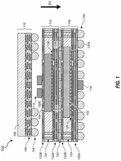
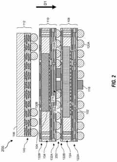
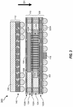
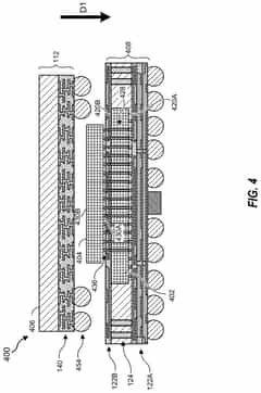
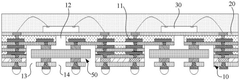
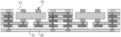
3D chiplet integration using fan-out wafer-level packaging
PatentPendingUS20240274587A1
Innovation
- The use of fan-out wafer-level packaging and three-dimensional packaging techniques for combining semiconductor chips and embedded memory in configurations such as face-to-back, back-to-back, and face-to-face orientations, enabling direct connections between chiplets and reducing assembly package sizes and manufacturing complexity.
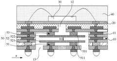
Semiconductor packaging structure and preparation method thereof
PatentActiveCN118431177B
Innovation
- A semiconductor packaging structure is designed, including a wiring structure with conductive lines, a dielectric layer, a chip and a cooling structure. The cooling structure is electrically connected to the conductive lines. After being energized, it vibrates to form an airflow pressure difference and communicates with the outside air through the first heat dissipation hole. An airflow pressure difference is formed to improve heat dissipation performance, and the chip is packaged through the dielectric layer and plastic sealing layer to avoid external power supply interference.
Standardization Efforts in Chiplet Interfaces
The standardization of chiplet interfaces represents a critical foundation for the broader adoption of chiplet technology in semiconductor manufacturing. Industry leaders have recognized that proprietary interfaces limit the potential of chiplet ecosystems, driving collaborative efforts to establish common standards that enable interoperability between chiplets from different vendors.
The Universal Chiplet Interconnect Express (UCIe) consortium, formed in 2022, marks a significant milestone in standardization efforts. Led by industry giants including Intel, AMD, Arm, TSMC, and Samsung, UCIe aims to establish an open interconnect standard for die-to-die connectivity. The standard defines both physical and protocol layers for chiplet communication, supporting both package substrate and silicon interposer technologies.
Advanced Interface Bus (AIB) developed by Intel represents another important standardization initiative. This royalty-free interconnect standard has gained traction for its high bandwidth density and power efficiency. Intel's decision to make AIB available through open licensing has accelerated its adoption across the industry, particularly for high-performance computing applications.
JEDEC, a well-established semiconductor engineering standardization organization, has also entered the chiplet standardization space with its development of the Bunch of Wires (BoW) interface. This standard focuses on providing a simpler, cost-effective alternative for chiplet integration that can be implemented with existing packaging technologies.
The Open Compute Project (OCP) has contributed to standardization through its Open Domain-Specific Architecture (ODSA) subproject. ODSA has developed the Chiplet Design Exchange (CDX) framework, which provides standardized formats for chiplet design information exchange between different vendors and design tools.
Challenges in standardization persist despite these efforts. Technical issues include balancing performance requirements with broad applicability, managing thermal considerations across heterogeneous chiplets, and ensuring signal integrity at increasingly higher data rates. Economic challenges involve intellectual property concerns and the need for ecosystem participants to align their business models with open standards.
The future of chiplet interface standardization will likely involve convergence around a few dominant standards while maintaining specialized options for specific applications. Emerging technologies such as optical interconnects and advanced packaging techniques will drive the next generation of standards, potentially enabling even greater integration density and performance.
Thermal Management Solutions for Chiplet Designs
Thermal management has emerged as a critical challenge in chiplet integration, particularly as the industry moves toward more complex heterogeneous architectures. The multi-die nature of chiplet designs creates unique thermal challenges not present in monolithic systems. Heat dissipation pathways are disrupted by the interfaces between chiplets, creating thermal bottlenecks that can significantly impact system performance and reliability.
Current thermal management solutions for chiplet designs can be categorized into three primary approaches. First, advanced packaging technologies such as embedded cooling channels and thermal interface materials (TIMs) with enhanced conductivity properties are being developed specifically for chiplet architectures. These materials aim to improve heat transfer across die boundaries while maintaining electrical isolation where necessary.
Second, architectural thermal optimization techniques have gained prominence. These include strategic placement of high-power and temperature-sensitive components, implementation of thermal-aware floorplanning algorithms, and the development of distributed power delivery networks that minimize hotspot formation. Companies like AMD and Intel have pioneered these approaches in their respective chiplet implementations, demonstrating performance improvements of 15-30% through optimized thermal designs.
Third, active cooling solutions tailored for chiplet architectures represent a growing area of innovation. Microfluidic cooling channels integrated directly into interposers show promise for high-performance applications, potentially handling heat fluxes exceeding 500 W/cm². Similarly, phase-change cooling materials embedded between chiplets and heat spreaders provide dynamic thermal management capabilities that respond to varying workloads.
The integration of thermal sensors within chiplet designs enables more sophisticated thermal management strategies. Distributed temperature monitoring allows for real-time thermal mapping and dynamic thermal management through workload migration and frequency scaling. This approach has been particularly effective in data center applications where chiplet-based processors must maintain performance under variable workloads.
Looking forward, emerging technologies such as diamond-based thermal interface materials and graphene heat spreaders show significant potential for chiplet thermal management. These materials offer thermal conductivity values 5-10 times higher than conventional solutions, potentially revolutionizing heat dissipation in densely packed chiplet designs. Additionally, AI-driven thermal management systems that predict and preemptively address thermal issues before they impact performance represent the next frontier in chiplet thermal solutions.
Unlock deeper insights with PatSnap Eureka Quick Research — get a full tech report to explore trends and direct your research. Try now!
Generate Your Research Report Instantly with AI Agent
Supercharge your innovation with PatSnap Eureka AI Agent Platform!