

How Chiplet Integration Complies with Advanced Technical Regulations
OCT 15, 20259 MIN READ
Generate Your Research Report Instantly with AI Agent
Patsnap Eureka helps you evaluate technical feasibility & market potential.
Chiplet Integration Background and Objectives
Chiplet integration represents a paradigm shift in semiconductor design and manufacturing, emerging as a response to the slowing of Moore's Law and the increasing challenges in traditional monolithic chip scaling. This approach involves disaggregating complex system-on-chip (SoC) designs into smaller functional blocks, or "chiplets," which are then integrated using advanced packaging technologies. The evolution of chiplet technology can be traced back to the early 2010s, with significant acceleration in development over the past five years as major semiconductor companies sought alternatives to traditional scaling methods.
The technical trajectory of chiplet integration has been shaped by the need for higher performance, lower power consumption, and reduced manufacturing costs in increasingly complex computing systems. As transistor scaling becomes more difficult and expensive, chiplet architecture offers a viable path forward by allowing the mixing and matching of components manufactured using different process nodes, thereby optimizing for both performance and cost.
The primary objective of chiplet integration is to achieve system-level performance and functionality comparable to or exceeding that of monolithic designs, while maintaining manufacturability and cost-effectiveness. This involves overcoming significant technical challenges in areas such as inter-chiplet communication, thermal management, and testing methodologies.
Regulatory compliance has become a critical consideration in chiplet development, particularly as international tensions have led to increased scrutiny of semiconductor technologies. Advanced technical regulations now govern aspects such as export controls, security features, and environmental impact, requiring chiplet designs to incorporate compliance measures from the earliest stages of development.
The global semiconductor industry is witnessing a convergence around chiplet standards, with initiatives like the Universal Chiplet Interconnect Express (UCIe) consortium working to establish common interfaces and protocols. These standardization efforts aim to create an ecosystem where chiplets from different vendors can interoperate seamlessly, while still meeting the stringent regulatory requirements of different jurisdictions.
Looking forward, chiplet integration is expected to enable new classes of high-performance computing systems, particularly in data centers, artificial intelligence, and edge computing applications. The technology roadmap suggests continued refinement of integration techniques, with particular emphasis on improving die-to-die interconnects, power delivery networks, and system-level optimization methodologies that can adapt to evolving regulatory frameworks across global markets.
Market Demand Analysis for Chiplet Technology
The global chiplet market is experiencing unprecedented growth, driven by the increasing demand for high-performance computing solutions across various industries. Market research indicates that the chiplet technology market is projected to grow at a compound annual growth rate of 40% through 2027, reaching significant market valuation as industries recognize the advantages of modular chip design over traditional monolithic approaches.
This surge in demand stems primarily from data centers and cloud service providers seeking more efficient computing architectures to handle exponentially growing workloads. These sectors require solutions that offer improved performance while managing thermal constraints and power consumption—challenges that chiplet technology directly addresses through its disaggregated approach.
Consumer electronics manufacturers represent another substantial market segment embracing chiplet technology. As devices become more sophisticated while maintaining form factor constraints, the ability to integrate specialized processing units through chiplet architecture provides significant competitive advantages. This is particularly evident in smartphones, tablets, and wearable technology where space optimization and power efficiency are paramount.
The automotive industry has emerged as a rapidly growing market for chiplet technology, particularly with the acceleration of autonomous driving systems and advanced driver assistance features. These applications demand high-performance computing capabilities with stringent reliability requirements that align well with chiplet integration approaches that can isolate critical functions.
Telecommunications infrastructure, especially with the ongoing global 5G rollout and preparation for 6G technologies, represents another significant market driver. Network equipment manufacturers are increasingly adopting chiplet-based designs to achieve the necessary processing capabilities while managing power and thermal constraints in dense deployment environments.
From a geographical perspective, North America and East Asia currently dominate the chiplet market demand, with Europe showing accelerated adoption rates. This regional distribution closely follows semiconductor manufacturing capabilities and technology development centers, though regulatory frameworks vary significantly across these regions.
The market demand is further characterized by increasing emphasis on compliance with technical regulations. As chiplet technology enables more complex systems-in-package, regulatory bodies worldwide are developing new frameworks to address security, reliability, and interoperability concerns. Companies that can navigate these evolving regulatory landscapes while delivering compliant chiplet solutions are positioned to capture premium market segments where certification requirements are stringent.
Industry analysts note that the chiplet market is transitioning from early adoption to mainstream implementation, with standardization efforts like Universal Chiplet Interconnect Express (UCIe) accelerating this shift by addressing interoperability concerns that previously limited market expansion.
Global Chiplet Technology Landscape and Challenges
The global chiplet technology landscape is experiencing rapid evolution, with significant advancements across North America, Asia, and Europe. Leading semiconductor companies like TSMC, Intel, AMD, and Samsung have established strong positions in chiplet development, creating a competitive environment that drives innovation. The United States maintains technological leadership through companies like Intel and AMD, while Taiwan dominates manufacturing through TSMC's advanced packaging solutions. China is aggressively investing in domestic chiplet capabilities to reduce dependency on foreign technologies amid geopolitical tensions.
The chiplet approach represents a paradigm shift from traditional monolithic chip design, allowing for the integration of multiple smaller dies into a single package. This modular architecture enables manufacturers to combine different process nodes, improving yield rates and reducing production costs. The Universal Chiplet Interconnect Express (UCIe) consortium, formed in 2022, marks a significant step toward standardization, though competing standards like TSMC's LIPINCON and Intel's AIB continue to fragment the ecosystem.
Technical challenges persist across multiple dimensions of chiplet integration. Thermal management becomes increasingly complex as multiple dies operate in close proximity, requiring sophisticated cooling solutions and thermal interface materials. Power delivery across chiplet boundaries presents significant design challenges, particularly for high-performance computing applications. Signal integrity issues arise from the increased number of interconnects between dies, necessitating advanced packaging technologies to maintain performance.
Regulatory compliance adds another layer of complexity to chiplet development. Export controls, particularly those imposed by the United States on advanced semiconductor technologies to China, create significant barriers to global collaboration. Different regions maintain varying standards for electromagnetic interference (EMI), reliability testing, and environmental compliance, complicating the development of globally marketable chiplet solutions.
Manufacturing challenges remain substantial, with known good die (KGD) testing being particularly problematic. Traditional testing methods designed for monolithic chips are insufficient for detecting defects in individual chiplets before integration, increasing the risk of yield loss during final assembly. Advanced packaging technologies like TSMC's CoWoS (Chip on Wafer on Substrate) and Intel's EMIB (Embedded Multi-die Interconnect Bridge) are evolving to address these challenges but require significant capital investment.
The industry faces a critical talent shortage in chiplet design and integration, with universities struggling to produce graduates with the interdisciplinary skills required for advanced packaging technologies. This human resource challenge, combined with the technical and regulatory hurdles, represents a significant constraint on the broader adoption of chiplet technology despite its promising benefits for semiconductor scaling beyond traditional Moore's Law limitations.
Current Chiplet Integration Solutions
01 Standardization and compliance frameworks for chiplet integration
Standardization frameworks and compliance protocols are essential for ensuring interoperability between chiplets from different vendors. These frameworks define electrical, physical, and logical interfaces that chiplets must adhere to for successful integration. Compliance testing methodologies verify that chiplets meet these standards, enabling seamless integration in heterogeneous systems while reducing integration risks and time-to-market.- Standardization and compliance frameworks for chiplet integration: Standardization frameworks and compliance protocols are essential for ensuring interoperability between chiplets from different manufacturers. These frameworks define electrical, physical, and logical interfaces that chiplets must adhere to for successful integration. Compliance testing methodologies verify that chiplets meet these standards, enabling seamless integration in heterogeneous systems while reducing compatibility issues and development costs.
- Testing and verification methods for chiplet compliance: Various testing and verification methods are employed to ensure chiplets comply with integration standards. These include automated test equipment for electrical parameter verification, thermal stress testing, signal integrity analysis, and functional validation. Advanced simulation tools model chiplet behavior before physical integration, while built-in self-test mechanisms enable continuous monitoring of compliance parameters during operation, ensuring reliable system performance.
- Interface technologies for compliant chiplet integration: Specialized interface technologies facilitate compliant chiplet integration across different platforms. These include high-bandwidth die-to-die interconnects, standardized I/O protocols, and physical connection mechanisms that ensure signal integrity. Advanced packaging technologies support these interfaces, including silicon interposers, organic substrates, and through-silicon vias (TSVs), which collectively enable high-performance, energy-efficient communication between chiplets while maintaining compliance with industry standards.
- Power management and thermal compliance in chiplet systems: Power management and thermal compliance are critical aspects of chiplet integration. Advanced techniques include dynamic voltage and frequency scaling specific to individual chiplets, thermal sensors for real-time monitoring, and intelligent power distribution networks. Compliance standards define acceptable power envelopes and thermal profiles that chiplets must maintain during operation, ensuring system stability and preventing thermal-induced failures in densely integrated multi-chiplet packages.
- Design for compliance in heterogeneous chiplet architectures: Design methodologies specifically tailored for compliance in heterogeneous chiplet architectures focus on ensuring seamless integration across different process nodes, manufacturers, and functional domains. These methodologies incorporate compliance verification at early design stages, standardized design rules, and parameterized interfaces that can adapt to various integration scenarios. EDA tools with compliance-checking capabilities help designers validate chiplet designs against established standards before fabrication, reducing integration risks and accelerating time-to-market.
02 Testing and validation methodologies for chiplet compliance
Specialized testing and validation methodologies are critical for verifying chiplet compliance with integration standards. These include automated test equipment, built-in self-test mechanisms, and validation protocols that assess signal integrity, power delivery, thermal performance, and functional compatibility. Comprehensive testing ensures that chiplets from different manufacturers can be reliably integrated while maintaining system performance and reliability requirements.Expand Specific Solutions03 Interface technologies for compliant chiplet integration
Advanced interface technologies enable compliant chiplet integration by providing standardized communication protocols between chiplets. These interfaces include die-to-die interconnects, through-silicon vias (TSVs), and advanced packaging technologies that support high-bandwidth, low-latency communication while maintaining signal integrity. Standardized interfaces ensure that chiplets from different vendors can communicate effectively within a single package, facilitating modular system design.Expand Specific Solutions04 Design tools and methodologies for chiplet compliance
Specialized design tools and methodologies support the development of compliant chiplets by providing verification capabilities, design rule checking, and simulation environments. These tools help designers ensure that their chiplets adhere to integration standards before fabrication, reducing development cycles and integration issues. Design methodologies include modular approaches that facilitate compliance with established chiplet integration frameworks.Expand Specific Solutions05 Power and thermal management for compliant chiplet integration
Power and thermal management techniques are crucial for ensuring chiplet compliance in integrated systems. These include standardized power delivery networks, thermal interface materials, and cooling solutions that maintain optimal operating conditions across multiple chiplets. Compliance standards for power distribution and thermal management ensure that chiplets can function reliably when integrated, preventing performance degradation and ensuring system reliability.Expand Specific Solutions
Key Industry Players in Chiplet Ecosystem
Chiplet integration technology is currently in a growth phase, with the market expanding rapidly due to increasing demand for advanced semiconductor solutions that comply with technical regulations. The global chiplet market is projected to reach significant scale as more companies adopt this modular approach to overcome traditional monolithic design limitations. From a technical maturity perspective, industry leaders like TSMC, Intel, and Huawei have made substantial progress in developing compliant chiplet technologies, while AMD (through partnerships) has successfully commercialized products. Companies including Micron, GlobalFoundries, and Fujitsu are advancing interconnect standards and packaging technologies. Emerging players such as MetaX and Hygon are focusing on specialized applications, indicating the technology's broadening adoption across the semiconductor ecosystem while addressing regulatory requirements through collaborative industry standards.
Taiwan Semiconductor Manufacturing Co., Ltd.
Technical Solution: TSMC has developed advanced chiplet integration technologies through its Integrated Fan-Out (InFO) and System on Integrated Chips (SoIC) platforms. Their approach focuses on providing high-bandwidth, low-latency interconnects between chiplets while maintaining compliance with technical regulations. TSMC's 3DFabric technology combines front-end and back-end innovations to enable both 2.5D and 3D chiplet integration. Their CoWoS (Chip-on-Wafer-on-Substrate) platform specifically addresses high-performance computing needs by integrating multiple chiplets on a silicon interposer. TSMC ensures regulatory compliance through comprehensive design rule checking systems that verify signal integrity, power integrity, and electromagnetic compatibility. Their advanced packaging technologies incorporate thermal solutions that meet international safety standards while enabling higher performance density. TSMC also provides customers with extensive design collateral to ensure chiplet designs meet various regional certification requirements.
Strengths: Industry-leading process technology enabling the most advanced chiplet implementations; comprehensive packaging portfolio supporting various integration approaches; established ecosystem with major fabless customers. Weaknesses: Higher manufacturing costs for advanced packaging solutions; complex supply chain coordination required for multi-vendor chiplet integration; thermal management challenges in densely packed configurations.
Huawei Technologies Co., Ltd.
Technical Solution: Huawei has developed a comprehensive chiplet integration strategy centered around their Kirin chipsets and custom interconnect technologies. Their approach focuses on disaggregating SoC designs to optimize performance, power efficiency, and manufacturing yield while ensuring compliance with technical regulations. Huawei's chiplet architecture employs a proprietary high-speed die-to-die interface that achieves data rates exceeding 8GT/s while maintaining signal integrity within regulatory limits. Their compliance strategy includes built-in self-test mechanisms that continuously monitor thermal conditions and electromagnetic emissions during operation. Huawei has implemented advanced power management techniques that dynamically adjust individual chiplet performance to stay within regulatory power envelopes. Their packaging technology incorporates specialized materials that enhance thermal dissipation while meeting international safety standards for consumer electronics. Despite facing export restrictions, Huawei continues to advance their chiplet technology through partnerships with domestic semiconductor companies and research institutions.
Strengths: Vertical integration allowing optimized chiplet designs across hardware and software; strong expertise in power-efficient mobile chipsets; established domestic supply chain relationships. Weaknesses: Limited access to advanced manufacturing technologies due to trade restrictions; potential interoperability challenges with global standards; reduced economies of scale compared to competitors with global market access.
Critical Patents and Technical Innovations
Technologies for a unified test and debug architecture
PatentWO2024205614A1
Innovation
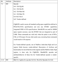
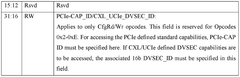
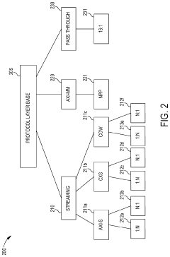
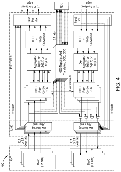
- A unified test and debug architecture is implemented using an external hardware debug interface that is interface-agnostic, employing Universal Chiplet Interconnect Express (UCIe) packets for debug messages, allowing for seamless communication and interoperability between chiplets, and enabling testing at various stages from sort stage to infield debugging.

Multi-use chip-to-chip interface
PatentActiveUS11892966B2
Innovation
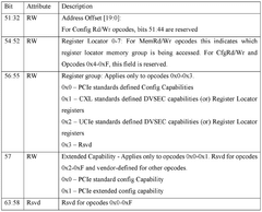
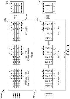
- Implementing a programmable chip-to-chip interface model that allows the anchor IC to dynamically adapt to various configurations and requirements of coupled components, enabling the anchor to connect with multiple chiplets at any port and reconfigure features and functions without hardware changes, using software programming to support different use cases and orientations.
Regulatory Compliance Framework for Chiplets
The regulatory landscape for chiplet technology is evolving rapidly as governments and international bodies recognize the strategic importance of semiconductor innovation. A comprehensive compliance framework for chiplets must address multiple regulatory domains including export controls, security standards, environmental regulations, and intellectual property protection. Current frameworks vary significantly across regions, with the United States implementing the CHIPS Act and export restrictions, the European Union focusing on the European Chips Act with sustainability requirements, and Asia-Pacific regions developing their own regulatory approaches.
Key components of an effective chiplet regulatory compliance framework include technical standards alignment, security certification processes, and environmental compliance mechanisms. Organizations such as IEEE, JEDEC, and UCIe Consortium have established foundational standards for chiplet interfaces and integration, which serve as technical benchmarks for regulatory compliance. These standards address critical aspects like electrical specifications, thermal management, and physical dimensions that directly impact regulatory requirements.
Security certification for chiplets presents unique challenges due to their disaggregated nature. Regulatory frameworks increasingly require comprehensive security validation across the entire chiplet ecosystem, including die-to-die interfaces and integration methodologies. The zero-trust security model is becoming a regulatory expectation, requiring manufacturers to implement robust authentication mechanisms between chiplet components.
Environmental compliance represents another critical dimension, with regulations like EU's RoHS and REACH directly impacting chiplet manufacturing processes. The framework must address material restrictions, energy efficiency requirements, and end-of-life considerations. Advanced packaging technologies used in chiplet integration must comply with increasingly stringent environmental standards regarding chemical usage and waste management.
Intellectual property protection within the chiplet ecosystem requires specialized regulatory approaches. The modular nature of chiplets creates complex IP ownership scenarios that traditional semiconductor IP frameworks struggle to address. Emerging regulations are beginning to recognize the need for new licensing models and protection mechanisms specific to chiplet-based designs.
Implementation of a robust compliance framework requires cross-functional collaboration between technical, legal, and business teams. Organizations must establish systematic processes for regulatory monitoring, compliance verification, and documentation. Leading semiconductor companies are developing specialized compliance management systems that track regulatory requirements across global markets and integrate compliance considerations into the chiplet design process from inception.
Cross-border Technology Transfer Considerations
Cross-border technology transfer in chiplet integration presents significant regulatory challenges that must be carefully navigated. The semiconductor industry's globalized supply chain means that chiplet technologies frequently cross international borders during development and production phases. Different countries maintain varying levels of export controls on advanced semiconductor technologies, with particular scrutiny applied to technologies with potential dual-use applications that could serve both civilian and military purposes.
The United States has implemented the CHIPS Act and strengthened Export Administration Regulations (EAR) specifically targeting advanced semiconductor technologies, including those related to chiplet integration. These regulations restrict the transfer of certain advanced packaging technologies to designated countries, requiring companies to obtain specific licenses for technology transfers. Similarly, the European Union has established the European Chips Act with provisions governing technology transfer of critical semiconductor technologies.
Asian technology powerhouses like Japan, South Korea, and Taiwan have implemented their own regulatory frameworks that impact chiplet technology transfers. Taiwan, as a major semiconductor manufacturing hub, has particularly stringent controls on technology outflow to maintain its competitive advantage in advanced packaging technologies.
Compliance with these cross-border regulations requires semiconductor companies to implement robust technology classification systems. This involves detailed documentation of technical specifications to determine which chiplet integration technologies fall under restricted categories. Companies must establish clear protocols for technology sharing with international partners and subsidiaries, including comprehensive training programs for technical staff on compliance requirements.
Intellectual property protection represents another critical dimension of cross-border technology transfer. Companies must develop strategies that balance IP protection with regulatory compliance, often requiring specialized legal expertise in international technology transfer law. This may involve creating technology licensing agreements that satisfy both commercial objectives and regulatory requirements across multiple jurisdictions.
The dynamic nature of international relations further complicates chiplet technology transfers. Geopolitical tensions can rapidly alter the regulatory landscape, requiring companies to maintain flexible compliance strategies. Industry consortia and international standards organizations play an increasingly important role in facilitating compliant technology transfers by establishing globally recognized standards for chiplet integration that satisfy regulatory requirements across multiple jurisdictions.
Unlock deeper insights with Patsnap Eureka Quick Research — get a full tech report to explore trends and direct your research. Try now!
Generate Your Research Report Instantly with AI Agent
Supercharge your innovation with Patsnap Eureka AI Agent Platform!