

Analyzing Chiplet Integration Materials for Semiconductor Advances
OCT 15, 20259 MIN READ
Generate Your Research Report Instantly with AI Agent
Patsnap Eureka helps you evaluate technical feasibility & market potential.
Chiplet Integration Materials Background and Objectives
Chiplet integration technology represents a paradigm shift in semiconductor design and manufacturing, moving away from monolithic system-on-chip (SoC) approaches toward modular architectures that combine multiple smaller dies (chiplets) into a single package. This evolution began in the mid-2010s as semiconductor manufacturers faced increasing challenges with traditional Moore's Law scaling. The physical limitations of silicon, rising manufacturing costs for advanced nodes, and yield concerns at smaller geometries collectively drove the industry toward chiplet-based designs as a viable alternative for continued performance improvements.
The materials used for chiplet integration play a critical role in determining the overall performance, reliability, and cost-effectiveness of advanced semiconductor packages. These materials must address several key functions: providing mechanical support, enabling electrical connections between chiplets, managing thermal dissipation, and ensuring signal integrity across the package. The historical progression of integration materials has evolved from simple organic substrates to advanced interposers incorporating through-silicon vias (TSVs), redistribution layers (RDLs), and sophisticated micro-bump technologies.
Current integration approaches primarily utilize silicon, glass, or organic interposers, each offering distinct advantages and limitations. Silicon interposers provide excellent dimensional stability and thermal matching but at higher costs. Organic interposers offer cost benefits but face limitations in wiring density and thermal performance. Glass interposers represent an emerging middle ground with promising electrical and thermal characteristics.
The primary technical objectives for advancing chiplet integration materials center on several critical parameters. First is the achievement of finer interconnect pitches to increase bandwidth density between chiplets. Current state-of-the-art interconnects operate at 40-55μm pitch, with industry roadmaps targeting sub-10μm pitches within the next five years. Second is the reduction of power consumption in the interconnect fabric, which currently represents a significant portion of system power budget in advanced packages.
Additional objectives include improving thermal management capabilities to handle increasing power densities, enhancing signal integrity for high-speed data transmission, and developing materials with coefficient of thermal expansion (CTE) values closely matched to silicon to minimize mechanical stress. Cost reduction remains a persistent goal, as current advanced packaging techniques can represent 30-40% of total manufacturing costs for high-performance computing applications.
The evolution of chiplet integration materials is closely aligned with broader semiconductor industry trends, including the push toward heterogeneous integration, 2.5D and 3D packaging architectures, and the growing importance of specialized computing for artificial intelligence and machine learning workloads. As these applications drive demand for ever-increasing computational density and energy efficiency, the development of advanced integration materials becomes increasingly critical to semiconductor innovation.
Market Demand Analysis for Advanced Semiconductor Packaging
The advanced semiconductor packaging market is experiencing unprecedented growth driven by the increasing demand for high-performance computing, artificial intelligence, 5G communications, and Internet of Things (IoT) applications. As traditional monolithic chip scaling approaches physical limitations described by Moore's Law, chiplet-based integration has emerged as a critical solution pathway for continued semiconductor advancement.
Market research indicates that the advanced packaging segment is projected to grow at a CAGR of 8.2% from 2023 to 2028, reaching a market value of $42 billion. Specifically, the chiplet integration materials market is expected to expand even faster, with estimates suggesting a 10.5% CAGR during the same period. This accelerated growth reflects the industry's pivot toward heterogeneous integration strategies.
Consumer electronics remains the largest application segment, accounting for approximately 35% of the advanced packaging market. However, data centers and high-performance computing applications are showing the fastest growth rates, driven by the exponential increase in computational demands for AI training and inference workloads.
Geographically, Asia-Pacific dominates the market with over 60% share, primarily due to the concentration of semiconductor manufacturing facilities in Taiwan, South Korea, and increasingly China. North America follows with approximately 20% market share, largely focused on design innovation and high-value applications.
The demand for advanced materials enabling chiplet integration is particularly strong. Silicon interposers, organic substrates, and advanced dielectrics are experiencing heightened demand as they form the foundation for chiplet-based architectures. Additionally, thermal interface materials are seeing increased adoption due to the higher thermal densities associated with tightly packed chiplet designs.
Industry surveys reveal that 78% of semiconductor manufacturers are actively investing in chiplet integration capabilities, with particular emphasis on materials that can support finer interconnect pitches and improved signal integrity. The market for high-bandwidth memory (HBM) integration solutions is growing at 15% annually, reflecting the critical need for memory-compute integration in data-intensive applications.
Customer requirements are evolving toward solutions that offer improved power efficiency, with 82% of end-users citing power consumption as a critical consideration. This has accelerated demand for advanced packaging materials that can support lower-power operation while maintaining performance targets.
Current State and Challenges in Chiplet Integration Materials
The global chiplet integration materials landscape is currently experiencing rapid evolution, with significant advancements in both research and commercial applications. Leading semiconductor manufacturers including TSMC, Intel, AMD, and Samsung have deployed various chiplet architectures in their high-performance products, demonstrating the technology's commercial viability. Current integration approaches primarily utilize silicon interposers, organic substrates, and advanced packaging technologies such as TSMC's CoWoS (Chip on Wafer on Substrate) and Intel's EMIB (Embedded Multi-die Interconnect Bridge).
Material science represents a critical challenge in chiplet integration, particularly regarding the development of interconnect materials that can maintain signal integrity while minimizing latency between dies. Current materials such as copper, aluminum, and increasingly cobalt face limitations in electrical conductivity at reduced dimensions. Research indicates that resistance increases exponentially as interconnect dimensions shrink below 10nm, creating significant power and thermal management challenges.
Thermal interface materials (TIMs) present another substantial hurdle, as chiplet architectures generate concentrated heat zones that require advanced thermal management solutions. Current materials including metal-based solders, polymer-based compounds, and emerging graphene-enhanced TIMs demonstrate varying levels of effectiveness, with thermal conductivity values ranging from 1-25 W/mK for conventional materials to potentially 100+ W/mK for next-generation solutions.
Mechanical stress management remains problematic due to coefficient of thermal expansion (CTE) mismatches between different materials in the chiplet stack. This mismatch can lead to warpage, delamination, and ultimately reliability failures. Current underfill materials and stress buffer layers provide partial solutions but require further optimization for increasingly complex 3D architectures.
Geographical distribution of chiplet integration technology development shows concentration in East Asia (Taiwan, South Korea, Japan), North America (USA), and Europe (Netherlands, Germany). TSMC and Intel lead in advanced packaging patents, with approximately 60% of relevant intellectual property concentrated among the top five semiconductor manufacturers.
Manufacturing scalability presents significant challenges, particularly in achieving cost-effective high-volume production with acceptable yields. Current die-to-die bonding techniques including thermal compression bonding and hybrid bonding face throughput limitations and require precise alignment tolerances below 1μm. Yield rates for complex chiplet packages currently range from 70-90%, significantly lower than monolithic designs, driving up effective production costs.
Standardization efforts remain fragmented despite initiatives like the Universal Chiplet Interconnect Express (UCIe) consortium. The lack of unified standards for physical interfaces, communication protocols, and testing methodologies impedes broader adoption across the semiconductor ecosystem and limits interoperability between chiplets from different manufacturers.
Current Technical Solutions for Chiplet Integration
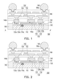
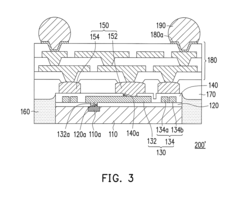
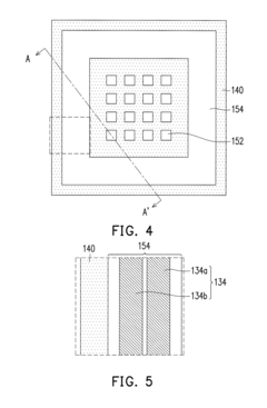
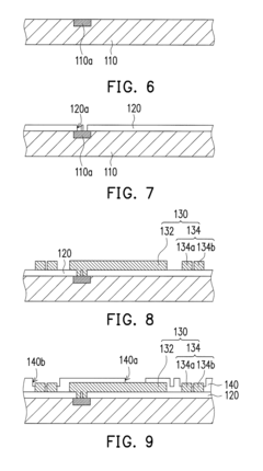
01 Advanced Interconnect Materials for Chiplet Integration
Various advanced materials are being developed for interconnecting chiplets in multi-die packages. These materials include specialized solders, copper pillars, and novel conductive adhesives that enable high-density connections between chiplets. These interconnect materials are designed to provide superior electrical performance, thermal conductivity, and mechanical reliability while accommodating the fine pitch requirements of modern chiplet architectures.- Advanced Interconnect Materials for Chiplet Integration: Various advanced materials are being developed for interconnecting chiplets in multi-die packages. These materials include specialized metals, alloys, and composite materials that provide superior electrical conductivity while maintaining thermal stability. These interconnect materials are crucial for ensuring reliable signal transmission between chiplets and can be applied using techniques such as micro-bumping, through-silicon vias (TSVs), and hybrid bonding technologies.
- Thermal Interface Materials for Chiplet Packages: Thermal management is critical in chiplet integration, requiring specialized thermal interface materials (TIMs) to efficiently dissipate heat from densely packed multi-die systems. These materials include advanced polymers, metal-infused compounds, and phase-change materials that provide optimal thermal conductivity between chiplets and heat spreaders. Effective thermal interface materials help maintain operational temperatures within acceptable ranges, improving overall system reliability and performance.
- Substrate and Interposer Materials for Chiplet Integration: Specialized substrate and interposer materials serve as the foundation for chiplet integration, providing mechanical support and electrical pathways between components. These materials include organic substrates, silicon interposers, glass carriers, and advanced ceramics that offer varying degrees of electrical performance, thermal management, and mechanical stability. The selection of appropriate substrate materials is crucial for achieving the desired balance between performance, reliability, and manufacturing cost in chiplet-based systems.
- Encapsulation and Underfill Materials for Chiplet Protection: Encapsulation and underfill materials provide physical protection and structural integrity to chiplet assemblies. These materials include specialized epoxies, silicones, and composite polymers that protect against environmental factors, mechanical stress, and thermal cycling. Advanced formulations offer improved adhesion, reduced coefficient of thermal expansion mismatch, and enhanced reliability for chiplet packages, while also facilitating heat dissipation and electrical insulation.
- Novel Bonding Technologies and Materials for Chiplet Assembly: Innovative bonding technologies and materials are being developed to enable more efficient and reliable chiplet integration. These include hybrid bonding materials, direct copper-to-copper bonding solutions, and low-temperature solders that facilitate fine-pitch connections between chiplets. These advanced bonding approaches allow for higher interconnect densities, improved electrical performance, and enhanced thermal characteristics, while potentially reducing manufacturing complexity and cost.
02 Thermal Interface Materials for Chiplet Packages
Thermal management is critical in chiplet integration, requiring specialized thermal interface materials (TIMs) to efficiently dissipate heat from densely packed multi-die systems. Advanced TIMs including phase-change materials, metal-based composites, and graphene-enhanced compounds are being developed to address the thermal challenges of chiplet architectures. These materials provide improved thermal conductivity while maintaining compatibility with various package types and assembly processes.Expand Specific Solutions03 Underfill and Encapsulation Materials for Chiplet Packages
Specialized underfill and encapsulation materials are essential for protecting chiplet interconnections and ensuring package reliability. These materials include low-viscosity underfills that can flow into the narrow gaps between chiplets, molding compounds with tailored coefficient of thermal expansion, and novel encapsulants that provide both mechanical protection and enhanced thermal performance. These materials are formulated to minimize stress on interconnects while providing environmental protection.Expand Specific Solutions04 Substrate and Interposer Materials for Chiplet Integration
Advanced substrate and interposer materials are being developed to support the complex routing requirements of chiplet-based designs. These include organic substrates with embedded traces, silicon and glass interposers with through-silicon vias (TSVs), and novel composite materials that combine the benefits of different substrate technologies. These materials provide the necessary electrical, thermal, and mechanical properties to support high-bandwidth communication between chiplets while maintaining package integrity.Expand Specific Solutions05 Novel Bonding Technologies for Chiplet Assembly
Innovative bonding technologies are being developed to enable precise alignment and attachment of chiplets in advanced packages. These include hybrid bonding techniques that combine metal-to-metal and dielectric-to-dielectric bonding, direct copper-to-copper bonding methods, and temporary bonding solutions that facilitate complex assembly processes. These technologies enable ultra-fine pitch connections between chiplets while ensuring high yield and reliability in the final integrated package.Expand Specific Solutions
Key Industry Players in Chiplet Integration Ecosystem
The chiplet integration materials market is currently in a growth phase, with increasing adoption driven by semiconductor scaling challenges. The market is expected to reach significant scale as chiplet architecture becomes mainstream in advanced semiconductor manufacturing. Leading players include TSMC, Samsung, and Intel, who have established mature chiplet integration technologies, while companies like SMIC, GlobalFoundries, and Micron are rapidly advancing their capabilities. Applied Materials and other equipment vendors provide critical manufacturing tools. The technology maturity varies across integration approaches, with 2.5D interposers being more established than emerging direct bonding techniques. Research partnerships between companies like IBM, IMEC, and universities are accelerating material innovations to address thermal management and interconnect density challenges.
Taiwan Semiconductor Manufacturing Co., Ltd.
Technical Solution: TSMC has pioneered advanced chiplet integration through their Chip-on-Wafer-on-Substrate (CoWoS) and System-on-Integrated-Chips (SoIC) technologies. Their CoWoS platform enables the integration of multiple chiplets on a silicon interposer with through-silicon vias (TSVs), providing high-bandwidth, low-latency connections between chiplets. TSMC's SoIC technology takes integration further with wafer-on-wafer and chip-on-wafer bonding techniques that achieve micron-level interconnect pitches. They've developed specialized dielectric materials and copper-to-copper hybrid bonding that creates connections with less than 10μm pitch[1]. TSMC has also innovated with their Integrated Fan-Out (InFO) packaging technology that eliminates the need for an interposer in some applications, reducing costs while maintaining high performance. Their materials research focuses on low-temperature bonding materials that minimize thermal stress during integration while maintaining electrical and mechanical integrity.
Strengths: Industry-leading process node capabilities (down to 3nm) that complement their advanced packaging; extensive experience with high-volume manufacturing of chiplet-based products; strong partnerships with major chip designers. Weaknesses: Higher cost structure compared to some competitors; capacity constraints during high demand periods; heavy dependence on specialized equipment suppliers for new packaging technologies.
Samsung Electronics Co., Ltd.
Technical Solution: Samsung has developed a comprehensive chiplet integration platform called I-Cube (Interposer-Cube) technology. This approach utilizes silicon interposers with fine-pitch TSVs to connect multiple chiplets in a single package. Samsung's latest iteration, I-Cube4, supports the integration of four HBM memory stacks with a logic chiplet. For the interposer material, Samsung has engineered specialized low-loss dielectrics that minimize signal degradation between chiplets. Their research has yielded copper pillar bump technology with pitches below 40μm, enabling higher interconnection density[2]. Samsung has also pioneered the use of hybrid bonding materials that can operate at lower temperatures (below 300°C) to reduce thermal stress during manufacturing. Their X-Cube technology employs direct bonding techniques with specialized surface preparation materials to achieve die-to-wafer and die-to-die connections with sub-10μm interconnect pitches. Samsung has additionally developed proprietary underfill materials that enhance thermal performance and reliability.
Strengths: Vertical integration across memory and logic manufacturing provides unique material optimization capabilities; strong R&D investment in advanced packaging; ability to leverage memory expertise for HBM integration. Weaknesses: Somewhat behind TSMC in high-volume production of the most advanced chiplet solutions; challenges in thermal management for high-performance computing applications; higher defect rates reported in early chiplet integration efforts.
Critical Materials Science Innovations for Chiplets
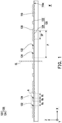
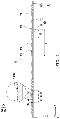
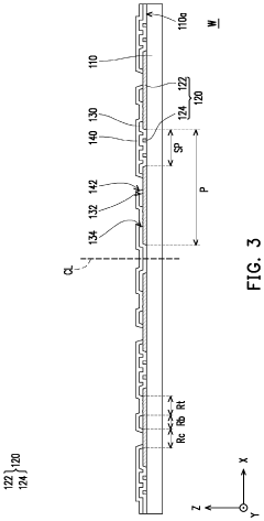
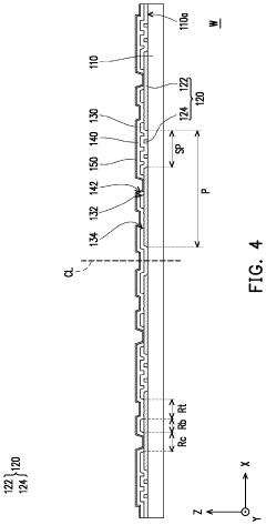
Integrated circuit component and package structure having the same
PatentPendingUS20240087967A1
Innovation
- The method involves forming conductive pads with specific structural configurations, including core, buffer, and testing regions, and using conductive vias to connect these pads, along with a passivation layer and seed layer formation, to enable reliable electrical testing and packaging, while optimizing the layout for reduced manufacturing costs.
Semicondcutor structure and semiconductor manufacturing process thereof
PatentActiveUS10062654B2
Innovation
- The semiconductor structure incorporates a seal ring structure and a ring barrier made of conductive materials, surrounded by a mold material, which prevents encapsulation by the molding compound and provides structural reinforcement, thereby protecting the integrated circuit component during the dicing process and enhancing operational reliability.
Thermal Management Considerations for Chiplet Designs
Thermal management has emerged as a critical challenge in chiplet-based semiconductor designs, particularly as integration densities increase and power requirements grow. The transition from monolithic architectures to disaggregated chiplet designs introduces new thermal considerations that must be addressed through innovative materials and cooling strategies.
The primary thermal challenge in chiplet integration stems from the increased power density at interconnect points between dies. These junction areas can create localized hotspots that exceed 100°C during operation, potentially compromising both performance and reliability. Traditional cooling solutions designed for monolithic architectures often prove inadequate for these heterogeneous integration scenarios.
Advanced thermal interface materials (TIMs) represent a crucial component in chiplet thermal management. Recent developments in metal-based TIMs incorporating silver, indium, and gallium alloys have demonstrated thermal conductivities exceeding 80 W/mK, significantly outperforming conventional polymer-based solutions. These materials provide superior heat dissipation at the critical die-to-die and die-to-package interfaces.
Liquid cooling technologies are increasingly being adapted for chiplet architectures, with microfluidic cooling channels integrated directly into interposer layers. This approach enables targeted cooling of high-power chiplets while maintaining thermal uniformity across the package. Research indicates that microfluidic cooling can reduce junction temperatures by up to 35% compared to conventional air cooling in high-performance computing applications.
The vertical integration dimension of chiplet designs introduces additional thermal complexities. Through-silicon vias (TSVs) and micro-bumps, while essential for electrical connectivity, can create thermal bottlenecks or, conversely, serve as thermal conduits when properly designed. Copper-filled TSVs with optimized geometries have demonstrated the ability to reduce thermal resistance by up to 40% compared to standard implementations.
Computational fluid dynamics (CFD) modeling has become indispensable for thermal management in chiplet designs. Advanced simulation tools now incorporate multi-physics capabilities that account for the complex interplay between electrical, mechanical, and thermal properties across heterogeneous materials and structures. These tools enable accurate prediction of thermal profiles before physical prototyping, significantly reducing design iterations.
Emerging technologies such as phase-change materials and graphene-based thermal solutions show particular promise for chiplet applications. Recent research demonstrates that graphene heat spreaders can achieve in-plane thermal conductivity exceeding 2000 W/mK, potentially revolutionizing heat distribution in laterally integrated chiplet packages. These materials are especially valuable for managing transient thermal loads in applications with variable computational demands.
Supply Chain Resilience for Critical Integration Materials
The semiconductor industry's reliance on specialized integration materials for chiplet technology creates significant supply chain vulnerabilities that require strategic management. Recent disruptions, including the COVID-19 pandemic and geopolitical tensions between major semiconductor-producing nations, have exposed critical weaknesses in the global supply network for advanced materials essential to chiplet integration. These materials, including specialized dielectrics, advanced bonding metals, and thermal interface materials, often originate from limited geographical sources with concentrated manufacturing capabilities.
Diversification strategies have emerged as a primary approach to enhancing supply chain resilience. Leading semiconductor manufacturers are establishing multiple sourcing arrangements for critical materials, particularly for advanced packaging substrates and high-purity metals used in die-to-die interconnects. Intel's recent $20 billion investment in expanding its manufacturing footprint represents an industry-wide trend toward reducing dependency on single-source suppliers.
Geographical redistribution of manufacturing capabilities presents another dimension of supply chain reinforcement. The CHIPS Act in the United States and similar initiatives in Europe aim to rebalance the global semiconductor ecosystem, which has historically been concentrated in East Asia. These programs specifically target materials production facilities alongside chip manufacturing, recognizing that integration materials represent a critical vulnerability in the semiconductor value chain.
Inventory management practices are evolving to accommodate the unique characteristics of chiplet integration materials. Companies are moving beyond just-in-time models toward strategic stockpiling of materials with limited shelf life or specialized handling requirements. Advanced analytics and AI-driven forecasting tools are being deployed to optimize these inventory positions against supply disruption risks.
Technological innovation itself serves as a resilience mechanism, with research focused on material substitution possibilities. Alternative bonding technologies that reduce dependence on rare metals and development of synthetic substitutes for naturally-sourced materials demonstrate how R&D can mitigate supply vulnerabilities. TSMC's research into copper-based alternatives to gold interconnects exemplifies this approach.
Collaborative industry frameworks are emerging to address systemic vulnerabilities. Consortia like the Semiconductor Climate Consortium are expanding their focus beyond environmental concerns to include supply chain resilience, establishing shared early warning systems for material shortages and coordinating industry-wide responses to disruptions. These collaborative approaches recognize that no single company can independently secure the complex supply networks required for advanced chiplet integration.
Unlock deeper insights with Patsnap Eureka Quick Research — get a full tech report to explore trends and direct your research. Try now!
Generate Your Research Report Instantly with AI Agent
Supercharge your innovation with Patsnap Eureka AI Agent Platform!