

How Chiplet Integration is Transforming Electronics Patents
OCT 15, 20259 MIN READ
Generate Your Research Report Instantly with AI Agent
Patsnap Eureka helps you evaluate technical feasibility & market potential.
Chiplet Integration Background and Objectives
Chiplet integration represents a paradigm shift in semiconductor design and manufacturing, evolving from traditional monolithic system-on-chip (SoC) approaches to a more modular architecture. This technological evolution began in the early 2010s as semiconductor manufacturers faced increasing challenges with Moore's Law, which had guided industry progress for decades. The fundamental concept involves disaggregating large, complex chips into smaller functional blocks (chiplets) that can be manufactured separately and then integrated using advanced packaging technologies.
The historical trajectory of chiplet technology can be traced back to multi-chip modules (MCMs) used in mainframe computers during the 1980s. However, modern chiplet integration emerged as a response to the physical limitations of silicon scaling and the exponential rise in manufacturing costs for advanced process nodes. By 2015, companies like AMD pioneered commercial chiplet implementations with their Zen architecture, demonstrating significant advantages in yield, cost, and performance.
The primary technical objectives of chiplet integration include overcoming the limitations of monolithic designs, enhancing manufacturing yields, enabling heterogeneous integration of components manufactured using different process technologies, and providing greater design flexibility. Additionally, chiplet approaches aim to reduce time-to-market for new products and allow more efficient use of silicon area.
From a patent landscape perspective, chiplet integration has triggered a significant transformation in intellectual property strategies. Early patents focused primarily on basic interconnect technologies and packaging methods. As the field matured, patent activities expanded to cover more sophisticated aspects including die-to-die interfaces, thermal management solutions, and power distribution networks across multiple chiplets.
Current technical trends in chiplet integration focus on standardization efforts, with initiatives like Universal Chiplet Interconnect Express (UCIe) gaining industry support. These standards aim to create an ecosystem where chiplets from different vendors can interoperate seamlessly, potentially revolutionizing the semiconductor supply chain and business models.
The evolution of chiplet technology is closely aligned with broader industry trends toward specialized computing architectures for applications like artificial intelligence, high-performance computing, and edge devices. This specialization drives the need for heterogeneous integration, where different functional blocks can be optimized independently and then combined into a single package.
Looking forward, chiplet integration aims to enable new system architectures that were previously impractical with monolithic designs, potentially reshaping the semiconductor industry's structure and competitive dynamics. The patent landscape will likely continue evolving as companies seek to protect innovations in chiplet design, manufacturing, testing, and integration methodologies.
Market Demand Analysis for Chiplet Technology
The global market for chiplet technology is experiencing unprecedented growth, driven by the increasing demand for high-performance computing solutions across multiple sectors. As traditional monolithic chip designs approach their physical and economic limits under Moore's Law, chiplet-based architectures have emerged as a compelling alternative that offers improved yield, cost efficiency, and performance scalability. Market research indicates that the chiplet market is projected to grow at a compound annual growth rate exceeding 40% through 2026, with the total addressable market expected to reach several billion dollars by mid-decade.
Consumer electronics represents the largest current market segment for chiplet technology, with smartphones, tablets, and personal computers increasingly incorporating modular chip designs to deliver enhanced performance while managing thermal constraints. The data center and cloud computing sector follows closely, where the need for specialized accelerators and high-bandwidth memory integration has made chiplet designs particularly attractive for hyperscalers seeking to optimize their infrastructure investments.
Automotive and industrial applications are rapidly emerging as high-growth segments for chiplet technology. Advanced driver-assistance systems (ADAS) and autonomous driving platforms require heterogeneous computing capabilities that can be efficiently delivered through chiplet-based architectures. Similarly, industrial automation systems benefit from the ability to integrate different process nodes and specialized IP blocks within a single package.
The market demand for chiplet technology is further amplified by several macroeconomic and industry-specific factors. Supply chain resilience has become a strategic priority for many organizations following recent disruptions, making the modular nature of chiplets appealing as it potentially allows for more flexible sourcing strategies. Additionally, growing concerns about energy efficiency in data centers and edge computing applications have positioned chiplets as an environmentally sustainable approach to semiconductor design.
Patent activity in the chiplet space reflects this surging market demand, with filing rates increasing dramatically since 2018. Major semiconductor companies have been aggressively building their intellectual property portfolios around chiplet integration technologies, interconnect standards, and packaging innovations. This patent landscape indicates strong industry confidence in the long-term market potential of chiplet-based solutions.
Regional analysis reveals that North America currently leads in chiplet technology adoption, followed by East Asia and Europe. However, the fastest growth is occurring in the Asia-Pacific region, where government initiatives to strengthen domestic semiconductor capabilities are accelerating investments in advanced packaging technologies, including chiplet integration platforms.
Current State and Challenges in Chiplet Integration
Chiplet integration technology has evolved significantly over the past decade, transforming from a theoretical concept to a commercial reality. Currently, major semiconductor companies including Intel, AMD, TSMC, and Samsung have deployed chiplet-based architectures in their high-performance computing products. The global adoption rate has accelerated since 2018, with a compound annual growth rate exceeding 35% in patent filings related to chiplet technologies.
The current state of chiplet integration is characterized by diverse technical approaches. The most prevalent methods include silicon interposers, organic substrates with advanced routing, and various die-to-die interconnect technologies. Silicon interposers dominate high-performance applications due to their superior interconnect density, while organic substrates offer cost advantages for less demanding applications. Recent advancements in 2.5D and 3D packaging have further expanded implementation options.
Despite significant progress, chiplet integration faces several critical challenges. Die-to-die interconnect bandwidth remains a primary bottleneck, with current solutions struggling to achieve the necessary data rates while maintaining power efficiency. Thermal management presents another substantial hurdle, as the concentration of multiple dies in close proximity creates hotspots that conventional cooling solutions cannot adequately address.
Manufacturing yield and testing complexity represent significant economic challenges. The known-good-die (KGD) problem persists, where defective chiplets can compromise entire multi-die packages. Current testing methodologies are insufficient for thoroughly evaluating chiplet-to-chiplet interactions before final assembly, resulting in yield losses that impact production economics.
Standardization remains fragmented across the industry. While initiatives like the Universal Chiplet Interconnect Express (UCIe) consortium have made progress toward establishing common interfaces, proprietary solutions still dominate the market. This fragmentation impedes the development of a truly open chiplet ecosystem where components from different vendors can seamlessly integrate.
Patent landscapes reveal geographical concentration of chiplet innovation. North America leads with approximately 42% of global patents, followed by East Asia (38%) and Europe (15%). China has demonstrated the fastest growth rate in chiplet-related patents over the past three years, increasing its share from 8% to 18% of new filings.
The regulatory environment adds another layer of complexity, with export controls and technology transfer restrictions increasingly affecting global collaboration in advanced semiconductor technologies. These geopolitical factors are reshaping research partnerships and commercial strategies in chiplet development, potentially leading to divergent technical standards in different regions.
Current Technical Solutions for Chiplet Integration
01 Chiplet interconnection technologies
Various interconnection technologies are used to integrate chiplets, including advanced packaging methods that enable high-bandwidth, low-latency communication between different chiplets. These technologies focus on creating reliable electrical connections between chiplets while maintaining signal integrity. Interconnection methods include through-silicon vias (TSVs), micro-bumps, and bridge technologies that facilitate die-to-die communication in multi-chiplet systems.- Chiplet interconnection technologies: Various interconnection technologies are used to integrate chiplets, including advanced packaging methods that enable high-bandwidth, low-latency communication between different chiplets. These technologies focus on creating reliable electrical connections between chiplets while maintaining signal integrity. Interconnection approaches include silicon interposers, bridge technologies, and direct bonding methods that facilitate the integration of heterogeneous chiplets manufactured using different process nodes.
- Thermal management for chiplet integration: Thermal management solutions for chiplet-based designs address the challenges of heat dissipation in densely packed multi-chiplet systems. These solutions include specialized thermal interface materials, integrated cooling structures, and thermal-aware placement strategies. Effective thermal management is critical for maintaining performance and reliability in high-performance computing applications that utilize chiplet architecture, as thermal issues can lead to performance degradation and reduced lifespan of the integrated system.
- Power delivery networks for chiplet systems: Advanced power delivery networks are designed specifically for chiplet-based architectures to ensure stable and efficient power distribution across multiple integrated dies. These networks incorporate innovative power management techniques, including fine-grained voltage regulation, power gating, and dynamic power allocation. The power delivery solutions address the unique challenges of supplying different voltage domains across heterogeneous chiplets while minimizing power loss and maintaining signal integrity.
- Testing and validation methodologies for chiplet integration: Specialized testing and validation methodologies have been developed to ensure the reliability and functionality of chiplet-based systems. These include pre-integration testing of individual chiplets, interface testing between chiplets, and system-level validation after integration. The methodologies address the unique challenges of testing complex multi-die systems, including known-good-die testing, boundary scan techniques, and built-in self-test capabilities that can identify defects in chiplet interfaces and interconnections.
- Design automation for chiplet-based systems: Electronic design automation tools and methodologies specifically tailored for chiplet-based architectures facilitate the design, verification, and optimization of multi-chiplet systems. These tools support partitioning of system functionality across multiple chiplets, optimization of chiplet placement and routing, and verification of inter-chiplet interfaces. Advanced design automation capabilities include chiplet-aware floor planning, signal integrity analysis across chiplet boundaries, and automated generation of test structures for chiplet interfaces.
02 Thermal management for chiplet integration
Thermal management solutions are critical for chiplet-based systems due to the high power density and heat generation in tightly packed multi-die packages. These solutions include specialized heat spreaders, thermal interface materials, and cooling structures designed specifically for chiplet architectures. Effective thermal management ensures optimal performance and reliability of integrated chiplet systems by preventing thermal throttling and maintaining operating temperatures within acceptable ranges.Expand Specific Solutions03 Chiplet testing and yield improvement
Testing methodologies and yield improvement techniques specific to chiplet-based designs address the challenges of ensuring functionality across multiple integrated dies. These approaches include pre-integration testing, known-good-die selection, and post-integration validation methods. Advanced testing strategies help identify defects early in the manufacturing process, improving overall yield and reducing costs in chiplet-based semiconductor production.Expand Specific Solutions04 Power delivery networks for chiplet architectures
Specialized power delivery networks are designed to meet the unique requirements of chiplet-based systems, addressing challenges such as voltage droop, power integrity, and efficient power distribution across multiple dies. These networks incorporate advanced power management techniques, including on-die voltage regulation, power domains, and optimized power routing strategies to ensure stable power delivery to all chiplets in the integrated system.Expand Specific Solutions05 Heterogeneous integration of chiplets
Heterogeneous integration involves combining chiplets manufactured using different process technologies or having different functionalities into a single package. This approach allows for optimizing each chiplet for its specific function while maintaining system-level integration. Techniques include advanced packaging platforms, interposer technologies, and standardized interfaces that enable chiplets from different sources or technologies to work together seamlessly in a single integrated system.Expand Specific Solutions
Key Players in Chiplet Integration Patent Landscape
Chiplet integration is transforming electronics patents in a rapidly evolving market currently in its growth phase. The global chiplet market is expanding significantly, with projections indicating substantial growth as the technology addresses scaling limitations in traditional monolithic designs. From a technical maturity perspective, industry leaders like Intel, AMD, and TSMC are at the forefront, having developed advanced packaging technologies and established significant patent portfolios. Companies including Micron Technology, Samsung Electronics, and Taiwan Semiconductor Manufacturing Co. are investing heavily in chiplet-related innovations, while newer entrants like AvicenaTech are focusing on specialized interconnect technologies. The competitive landscape shows established semiconductor giants leveraging their manufacturing expertise while specialized firms target niche applications, creating a dynamic patent environment characterized by strategic partnerships and cross-licensing agreements.
Micron Technology, Inc.
Technical Solution: Micron has developed chiplet integration technologies specifically optimized for memory applications, including their Hybrid Memory Cube (HMC) and subsequent memory architectures. Their approach stacks multiple DRAM dies vertically using through-silicon vias (TSVs), with a logic chiplet at the base handling memory controllers and interfaces. Micron's patent portfolio covers specialized interconnect technologies for memory-to-logic chiplet communication, power management techniques for stacked memory dies, and thermal solutions for high-density memory configurations. Their patents also address testing methodologies for memory chiplets and yield optimization techniques[4][9]. Recent innovations include patents for heterogeneous memory integration, combining different memory types (DRAM, NAND, emerging memories) as separate chiplets within a single package. Micron has also patented techniques for chiplet-based Compute-in-Memory architectures, where processing elements are integrated alongside memory chiplets to reduce data movement and improve energy efficiency for AI workloads[10].
Strengths: Specialized expertise in memory chiplet integration; vertical integration capabilities from design to manufacturing; innovations in memory-specific interconnect technologies. Weaknesses: Narrower focus primarily on memory applications; faces competition from other memory manufacturers adopting similar approaches; challenges in scaling bandwidth proportionally with capacity increases.
Advanced Micro Devices, Inc.
Technical Solution: AMD pioneered commercial chiplet implementation with its Zen architecture, utilizing their proprietary Infinity Fabric interconnect technology. This approach allows AMD to mix and match different chiplets manufactured on optimal process nodes, creating a heterogeneous integration system. Their patent portfolio includes innovations in die-to-die communication protocols, thermal management across multiple chiplets, and power distribution networks. AMD's EPYC server processors incorporate up to 9 chiplets (8 CPU dies and 1 I/O die) interconnected via their Infinity Fabric, enabling scalable performance while maintaining manufacturing yield advantages[1][3]. Recent patents focus on enhancing inter-chiplet bandwidth, reducing latency, and implementing advanced power management techniques across multiple dies. AMD has also developed patents for chiplet-based GPU architectures following their acquisition of Xilinx, leveraging expertise in both CPU and FPGA chiplet implementations[5].
Strengths: Mature implementation with proven market success; excellent yield management through smaller die sizes; flexible product segmentation. Weaknesses: Proprietary interconnect standards may limit industry-wide adoption; inter-chiplet communication introduces latency penalties compared to monolithic designs; thermal challenges across multiple dies require complex cooling solutions.
Core Patent Analysis in Chiplet Integration
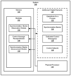
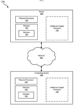
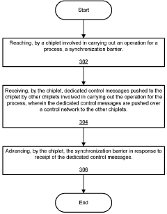
Systems and methods for chiplet synchronization
PatentWO2024130125A1
Innovation
- Implementing a parallel on-chip control network with dedicated control messages and a push mechanism, where chiplets maintain counters for each other and advance a synchronization barrier upon receipt of messages, reducing traffic on the control network and avoiding hardwired connections.
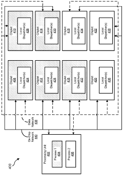
Edge interface placements to enable chiplet rotation into multi-chiplet cluster
PatentActiveUS12021062B2
Innovation
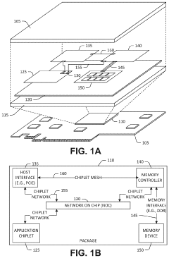
- The implementation of a chiplet architecture that uses a network-on-chip (NOC) with a chiplet protocol interface (CPI) to facilitate high-speed, flexible inter-chiplet communication, combined with a tightly packed matrix arrangement of chiplets and micro-bump interconnects to minimize latency and energy consumption.
IP Strategy and Patent Portfolio Management
In the rapidly evolving landscape of semiconductor technology, chiplet integration has fundamentally transformed intellectual property strategies and patent portfolio management approaches. Companies must now develop comprehensive IP strategies that address the unique challenges posed by this modular design paradigm. The fragmentation of traditional monolithic designs into multiple chiplets creates complex IP ownership scenarios, requiring organizations to carefully map their patent portfolios against emerging chiplet architectures.
Strategic patent filing has become increasingly important, with leading semiconductor companies focusing on three critical areas: interconnect technologies, integration methodologies, and system-level optimization. These areas represent the highest value IP in the chiplet ecosystem, as they enable the fundamental benefits of modular chip design. Companies like Intel, AMD, and TSMC have significantly increased their patent filings in these domains, creating defensive positions around their chiplet implementation approaches.
Cross-licensing agreements have emerged as essential tools in chiplet-based semiconductor development. The inherently collaborative nature of chiplet integration, where components from multiple vendors may be combined into a single package, necessitates clear IP frameworks. Industry leaders are establishing patent pools and licensing consortia specifically focused on chiplet integration standards, enabling broader adoption while protecting core innovations.
Patent landscaping has become more sophisticated in response to chiplet technology. Organizations now conduct multi-dimensional analyses that consider not only the technical aspects of chiplet designs but also the business relationships between potential partners and competitors. This approach helps identify strategic acquisition targets, licensing opportunities, and potential infringement risks across the fragmented supply chain.
Defensive patenting strategies have evolved to protect chiplet implementation methodologies. Companies are creating patent thickets around their specific integration approaches, packaging technologies, and testing methodologies. These defensive portfolios serve as barriers to competitors while simultaneously creating valuable assets for cross-licensing negotiations with ecosystem partners.
The internationalization of patent protection has accelerated, with companies filing chiplet-related patents across multiple jurisdictions to secure global protection. This trend reflects the distributed nature of semiconductor manufacturing and the global supply chains that support chiplet-based products. Strategic geographic coverage has become a critical consideration in portfolio management, with particular emphasis on regions with strong semiconductor manufacturing capabilities.
Standardization Efforts in Chiplet Ecosystem
The standardization of chiplet interfaces and protocols represents a critical foundation for the chiplet ecosystem's growth and widespread adoption. Industry consortia such as the Universal Chiplet Interconnect Express (UCIe) have emerged as pivotal forces in establishing common frameworks that enable interoperability between chiplets from different manufacturers. UCIe's 2022 specification release marked a watershed moment, defining both die-to-die and package-to-package interconnects with standardized physical layers, protocols, and power management features.
JEDEC and Open Compute Project have similarly contributed significant standardization efforts, focusing on memory interfaces and open hardware specifications respectively. These initiatives are collectively reducing fragmentation in the chiplet marketplace and accelerating innovation cycles by allowing designers to focus on core functionality rather than interface compatibility.
Patent landscapes reflect this standardization trend, with a notable increase in intellectual property filings related to chiplet interface technologies that align with emerging standards. Companies are strategically positioning their patent portfolios to both contribute to and benefit from standardization while maintaining competitive advantages in implementation-specific innovations.
The Chiplet Design Exchange (CDX) initiative represents another important standardization effort, focusing on creating common design methodologies and verification procedures. This approach addresses the complex challenge of ensuring chiplets from diverse sources can be reliably integrated into cohesive systems-in-package.
Standardization efforts extend beyond electrical interfaces to thermal management protocols, physical dimensions, and testing methodologies. The Advanced Interface Bus (AIB) and High Bandwidth Memory (HBM) standards exemplify how specialized interconnect technologies are being formalized to address specific performance requirements within the broader chiplet ecosystem.
Cross-industry collaboration has proven essential to successful standardization, with semiconductor manufacturers, electronic design automation companies, and systems integrators participating in joint development of specifications. This collaborative approach ensures standards address real-world implementation challenges while supporting innovation.
The patent implications of these standardization efforts are significant, with companies increasingly filing for protection on technologies that enhance or extend standard implementations rather than fundamental interface designs. This shift represents a maturation of the chiplet patent landscape toward value-added innovations that operate within standardized frameworks.
Unlock deeper insights with Patsnap Eureka Quick Research — get a full tech report to explore trends and direct your research. Try now!
Generate Your Research Report Instantly with AI Agent
Supercharge your innovation with Patsnap Eureka AI Agent Platform!