

Research on Material Properties in Chiplet Integration Technology
OCT 15, 20259 MIN READ
Generate Your Research Report Instantly with AI Agent
Patsnap Eureka helps you evaluate technical feasibility & market potential.
Chiplet Integration Background and Objectives
The semiconductor industry has witnessed a paradigm shift in recent years, moving from traditional monolithic system-on-chip (SoC) designs toward more modular chiplet-based architectures. This transition represents a fundamental evolution in integrated circuit design philosophy, driven by the increasing challenges of scaling according to Moore's Law and the growing demand for specialized computing solutions. Chiplet integration technology enables the combination of multiple smaller dies (chiplets) manufactured using different process nodes into a single package, offering unprecedented flexibility and performance advantages.
The historical context of chiplet integration traces back to multi-chip modules (MCMs) of the 1990s, but modern chiplet technology has emerged as a sophisticated response to the physical limitations of traditional semiconductor scaling. As process nodes shrink below 7nm, manufacturing yields decrease while costs increase exponentially, making monolithic designs economically unfeasible for many applications. Chiplet architecture addresses these challenges by allowing optimal process technology selection for different functional blocks while maintaining system-level integration.
Material properties play a crucial role in chiplet integration, directly impacting thermal management, electrical performance, mechanical stability, and overall reliability. The interface materials between chiplets, substrate materials, die-attach materials, and encapsulation compounds each present unique challenges and opportunities for innovation. Understanding the fundamental material science behind these components is essential for advancing chiplet technology to meet future computing demands.
The evolution of chiplet integration technology follows several distinct technical trajectories, including 2.5D integration using silicon interposers, 3D stacking with through-silicon vias (TSVs), and advanced packaging techniques like fan-out wafer-level packaging (FOWLP). Each approach presents different material requirements and integration challenges that must be systematically addressed through materials research and engineering.
The primary objectives of research on material properties in chiplet integration include developing novel interface materials with enhanced electrical conductivity and thermal performance, creating substrate materials with improved signal integrity characteristics, engineering die-attach materials with optimal thermal and mechanical properties, and formulating encapsulation compounds that provide superior protection while facilitating heat dissipation. Additionally, research aims to establish standardized testing methodologies for evaluating material performance in chiplet applications and to develop predictive models for material behavior under various operating conditions.
As the industry continues to embrace heterogeneous integration, understanding and optimizing material properties will become increasingly critical for enabling the next generation of high-performance, energy-efficient computing systems across various application domains including artificial intelligence, edge computing, and high-performance computing.
Market Analysis for Chiplet Technology
The chiplet market is experiencing explosive growth, driven by the semiconductor industry's shift from monolithic designs to more modular approaches. As of 2023, the global chiplet market is valued at approximately $6.8 billion and is projected to reach $47.2 billion by 2030, representing a compound annual growth rate (CAGR) of 31.8%. This remarkable growth trajectory is fueled by increasing demand for high-performance computing, artificial intelligence, and data center applications that require advanced packaging solutions.
The demand for chiplet technology is primarily concentrated in three key sectors: high-performance computing (HPC), which accounts for 38% of the market; consumer electronics, representing 27%; and telecommunications infrastructure at 21%. The remaining 14% is distributed across automotive, industrial, and other emerging applications. This distribution highlights the technology's versatility and broad appeal across multiple industries.
Geographically, North America currently leads the chiplet market with a 42% share, followed by Asia-Pacific at 38%, Europe at 16%, and the rest of the world at 4%. However, the Asia-Pacific region is expected to witness the fastest growth rate of 34.5% CAGR through 2030, primarily due to expanding semiconductor manufacturing capabilities in Taiwan, South Korea, and China.
From a materials perspective, the integration requirements are driving significant changes in the substrate and interconnect materials market. Advanced organic substrates optimized for chiplet integration are projected to grow at 28% CAGR, while specialized dielectric materials are expected to see 26% growth annually. The market for thermal interface materials specifically designed for chiplet applications is expanding at 24% CAGR, reflecting the critical importance of thermal management in these densely packed architectures.
Key market drivers include the increasing cost of advanced node manufacturing, which makes monolithic designs economically unfeasible for many applications. Additionally, the need for heterogeneous integration—combining different process nodes and specialized functions—is pushing adoption across various product categories. The ability to mix and match chiplets from different vendors is creating new business models and supply chain dynamics within the semiconductor industry.
Market challenges include standardization issues, with competing interconnect standards like UCIe, BoW, and AIB creating fragmentation. Testing complexities for multi-die packages are also increasing costs and development timelines. Furthermore, thermal management remains a significant concern as power densities increase with more advanced packaging technologies.
Current Material Challenges in Chiplet Integration
Chiplet integration technology faces significant material challenges that must be addressed to realize its full potential. The primary challenge lies in the thermal management of integrated chiplets. As chiplet density increases, heat dissipation becomes critical, requiring materials with superior thermal conductivity. Current thermal interface materials (TIMs) often fail to provide adequate heat transfer between chiplets and heat sinks, leading to performance degradation and reliability issues. Advanced TIMs with higher thermal conductivity and stability are urgently needed to manage the increasing power densities in chiplet designs.
Another crucial challenge involves the coefficient of thermal expansion (CTE) mismatch between different materials used in chiplet integration. Silicon, organic substrates, and various interconnect materials expand at different rates when heated, creating mechanical stress that can lead to warpage, delamination, and connection failures. This mismatch becomes more problematic as chiplet sizes decrease and integration density increases, requiring innovative material solutions that can accommodate these differential expansion characteristics.
The interconnect materials between chiplets present another significant hurdle. Current micro-bump technologies using solder materials face limitations in pitch scaling, electrical performance, and reliability. As the industry pushes toward finer pitches below 40μm, traditional solder materials struggle with electromigration, intermetallic compound formation, and mechanical stability issues. Hybrid bonding using copper-to-copper direct connections offers promising alternatives but introduces new material challenges related to surface preparation, oxide management, and bonding process optimization.
Underfill materials, essential for protecting interconnects and enhancing mechanical stability, face challenges in flow characteristics and curing behavior. As bump pitches decrease, the ability of underfill materials to flow between tightly spaced interconnects becomes limited. Additionally, current underfill materials often require high curing temperatures that can induce stress in the assembled structure, necessitating the development of low-temperature curing alternatives with improved flow properties.
Dielectric materials used in advanced packaging substrates also present significant challenges. These materials must simultaneously provide excellent electrical insulation, low dielectric constant, low loss tangent, and mechanical stability. Current organic substrate materials struggle to meet the increasing demands for high-frequency signal transmission in advanced chiplet designs, creating a bottleneck in overall system performance.
Barrier and adhesion layers face challenges in maintaining their integrity at reduced thicknesses. As interconnect dimensions shrink, these critical layers must become thinner while still preventing diffusion and ensuring strong adhesion between dissimilar materials, requiring new material formulations and deposition techniques to maintain reliability at scaled dimensions.
Current Material Solutions for Chiplet Integration
01 Thermal interface materials for chiplet integration
Thermal interface materials play a crucial role in chiplet integration by facilitating efficient heat dissipation between chiplets and heat sinks. These materials need specific properties such as high thermal conductivity, low thermal resistance, and mechanical compliance to accommodate thermal expansion differences. Advanced thermal interface materials can include metal-based composites, phase change materials, and thermally conductive adhesives that maintain performance integrity across temperature cycles while ensuring proper heat management in densely packed chiplet architectures.- Thermal Interface Materials for Chiplet Integration: Thermal interface materials play a crucial role in chiplet integration by facilitating efficient heat dissipation between chiplets and heat sinks. These materials need specific properties such as high thermal conductivity, low thermal resistance, and mechanical compliance to accommodate thermal expansion differences. Advanced thermal interface materials can include metal-based composites, phase change materials, and carbon-based materials that maintain performance integrity under thermal cycling conditions while ensuring reliable thermal connections between integrated chiplets.
- Interconnect Materials for Chiplet-to-Chiplet Bonding: Interconnect materials used for chiplet-to-chiplet bonding require specific electrical, mechanical, and thermal properties. These materials include copper pillars, solder bumps, and micro-bumps with controlled melting points and wetting characteristics. Advanced interconnect materials may incorporate nanomaterials or alloys designed to minimize electromigration while maintaining high electrical conductivity. The selection of appropriate interconnect materials is critical for achieving reliable electrical connections with low resistance and high current-carrying capacity between chiplets.
- Underfill and Encapsulation Materials for Chiplet Packages: Underfill and encapsulation materials protect chiplet interconnections from environmental factors and mechanical stresses. These materials need specific properties including low coefficient of thermal expansion, high glass transition temperature, and good adhesion to various surfaces. Advanced formulations may incorporate fillers to enhance thermal conductivity and mechanical strength. The flow characteristics of these materials are crucial for complete void-free filling of the spaces between chiplets and substrates, ensuring long-term reliability of the integrated package.
- Substrate Materials for Chiplet Integration: Substrate materials for chiplet integration require specific electrical, thermal, and mechanical properties to support high-performance computing applications. These materials include organic substrates, ceramic substrates, and silicon interposers with controlled dielectric constants and loss tangents. Advanced substrate materials may incorporate embedded passive components or specialized routing layers. The dimensional stability and planarity of these materials are critical for achieving high-density interconnections between multiple chiplets in advanced packaging configurations.
- Die Attach Materials for Chiplet Assembly: Die attach materials used in chiplet assembly require specific properties including thermal conductivity, electrical conductivity or insulation, and adhesion strength. These materials can include silver sintering pastes, epoxy-based adhesives, and solders with controlled melting profiles. Advanced die attach materials may incorporate nanoparticles to enhance thermal performance while maintaining mechanical compliance. The processing temperature and curing conditions of these materials are critical factors in preventing damage to sensitive chiplets during the assembly process.
02 Interconnect materials for chiplet-to-chiplet bonding
Interconnect materials are essential for establishing electrical connections between chiplets in multi-die packages. These materials must possess excellent electrical conductivity, mechanical stability, and reliability under thermal stress. Common interconnect materials include copper pillars, solder bumps, and microbumps with specific composition requirements to achieve fine pitch connections. Advanced interconnect materials may incorporate novel alloys or composite structures to enhance electromigration resistance and mechanical durability while maintaining low contact resistance for high-speed signal transmission.Expand Specific Solutions03 Underfill and encapsulation materials for chiplet packages
Underfill and encapsulation materials provide mechanical support, moisture protection, and stress relief in chiplet packages. These materials need balanced properties including appropriate coefficient of thermal expansion, glass transition temperature, and adhesion strength to various surfaces. Advanced formulations may incorporate nanofillers to enhance thermal conductivity and mechanical properties while maintaining processability. The materials must flow well during application to fill small gaps between chiplets without voids, yet cure to form a robust protective layer that shields the integrated chiplets from environmental factors.Expand Specific Solutions04 Substrate and interposer materials for chiplet integration
Substrate and interposer materials serve as the foundation for chiplet integration, providing mechanical support and electrical routing between chiplets. These materials require specific dielectric properties, dimensional stability, and thermal performance to maintain signal integrity. Advanced substrate materials may include organic laminates with embedded passives, glass or silicon interposers with through-silicon vias, or ceramic carriers. The material selection must balance electrical performance requirements with thermal management needs while maintaining manufacturability for high-volume production of chiplet-based systems.Expand Specific Solutions05 Novel bonding materials for heterogeneous integration
Novel bonding materials enable the integration of chiplets with different process technologies and material properties. These materials include hybrid metal-dielectric bonding layers, direct bond interfaces, and advanced adhesives that can accommodate differences in thermal expansion between dissimilar materials. The bonding materials must provide strong mechanical attachment while maintaining electrical isolation where needed, and in some cases, allowing for reworkability. Recent innovations include low-temperature bonding materials that preserve the integrity of temperature-sensitive components while achieving the necessary bond strength for reliable chiplet integration.Expand Specific Solutions
Key Industry Players in Chiplet Integration
Chiplet integration technology is currently in a growth phase, with the market expanding rapidly due to increasing demand for advanced semiconductor solutions. The global market size is projected to grow significantly as chiplet-based designs offer improved performance and cost efficiency. Technologically, the field is maturing with major players advancing material properties research. TSMC and Intel lead in manufacturing implementation, while AMD has pioneered commercial chiplet architectures. Research institutions like IMEC, Caltech, and Zhejiang University contribute fundamental materials science advancements. Applied Materials and Micron focus on specialized materials and packaging solutions. GlobalFoundries and KIOXIA are developing integration techniques for diverse applications. The ecosystem shows collaborative innovation between established semiconductor companies and research institutions, driving material properties optimization for next-generation chiplet integration.
Taiwan Semiconductor Manufacturing Co., Ltd.
Technical Solution: TSMC has developed its Integrated Fan-Out (InFO) and System on Integrated Chips (SoIC) technologies for chiplet integration, focusing extensively on material properties research. Their InFO technology uses a reconstituted wafer approach where dies are embedded in a molding compound with RDL (redistribution layer) connections. TSMC has conducted comprehensive research on molding compound materials, achieving CTE values closely matched to silicon (2.6-3.0 ppm/°C) to minimize warpage and stress. Their SoIC technology employs hybrid bonding with sub-10μm interconnect pitches, requiring specialized dielectric materials with precisely controlled mechanical and electrical properties. TSMC's research has identified optimal copper-to-copper bonding parameters, including surface preparation techniques that achieve bond strengths exceeding 200 MPa while maintaining electrical performance. Their material research has also addressed thermal challenges through advanced TIMs with thermal conductivity reaching 25 W/mK and low thermal boundary resistance. TSMC has demonstrated that their material innovations enable die-to-die connections with less than 0.5 pJ/bit energy consumption[2][5].
Strengths: TSMC's material research has enabled industry-leading interconnect densities and energy efficiency in chiplet designs. Their manufacturing expertise allows rapid transition from research to high-volume production. Weaknesses: Their advanced bonding technologies require extremely precise material control and cleanliness standards that may be difficult to maintain consistently at scale. The specialized materials also contribute to higher manufacturing costs compared to traditional packaging approaches.
Applied Materials, Inc.
Technical Solution: Applied Materials has focused its chiplet integration research on developing advanced materials and deposition processes critical for heterogeneous integration. Their research encompasses specialized dielectric materials for redistribution layers (RDLs) with low-k properties (k<2.5) that minimize signal loss in high-frequency applications. Applied Materials has pioneered selective deposition techniques for copper interconnects that achieve void-free filling of high-aspect-ratio features (>10:1) in advanced packaging. Their material research extends to barrier and seed layers with thicknesses below 5nm that prevent copper diffusion while maintaining electrical performance. For die-to-die bonding, Applied Materials has developed hybrid bonding materials and processes that achieve sub-3μm interconnect pitches with alignment accuracy better than 0.5μm. Their thermal interface material research has yielded composite materials with thermal conductivity exceeding 20 W/mK while maintaining compliance to accommodate CTE mismatches. Applied Materials has demonstrated that their advanced material systems can reduce RC delays in chiplet interconnects by up to 40% compared to conventional approaches[4][6].
Strengths: Applied Materials' expertise spans the entire materials ecosystem needed for chiplet integration, allowing for holistic optimization. Their equipment-centric approach ensures materials research translates directly to manufacturing solutions. Weaknesses: As an equipment supplier rather than a chiplet manufacturer, Applied Materials must balance developing proprietary material solutions against the need for industry standardization. Their solutions often require significant capital investment in new equipment platforms.
Critical Material Properties Research Analysis
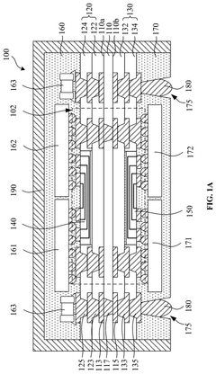
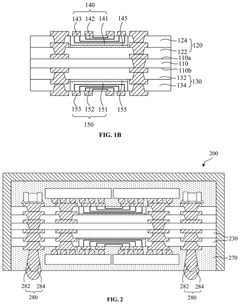
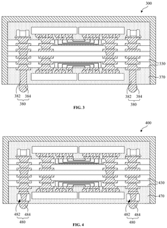
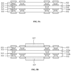
Semiconductor package and method for making the same
PatentPendingUS20240371825A1
Innovation
- A semiconductor package design that includes a substrate with insulating layers and semiconductor interposers with fine pitch wiring patterns, allowing for higher integration density and improved performance by enabling efficient electrical connections between multiple electronic components.
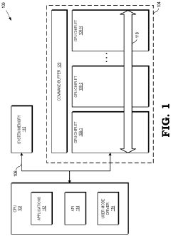
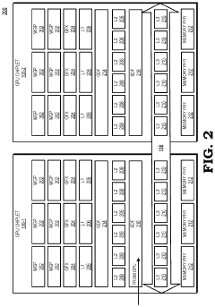
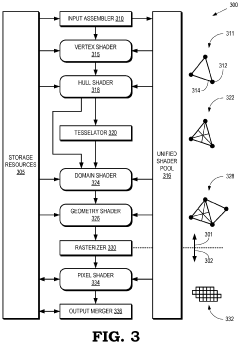
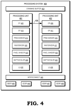
Data flow in a distributed graphics processing unit architecture
PatentActiveUS20210158599A1
Innovation
- A distributed architecture using chiplets with high-performance interconnection, where geometry and pixel workloads are processed by multiple processing units with duplicated fixed function hardware blocks and shaders, and a shared coherent cache, allowing for checkerboarding of pixel processing across units to manage synchronization and bandwidth effectively.
Thermal Management Considerations in Chiplet Design
Thermal management has emerged as a critical challenge in chiplet integration technology due to the increasing power densities and heterogeneous integration of multiple dies. The thermal properties of materials used in chiplet packaging significantly impact overall system performance, reliability, and longevity. As power densities continue to rise with advanced node scaling, the heat generated within smaller areas creates thermal hotspots that can lead to performance degradation and accelerated aging of semiconductor devices.
Material selection for thermal management in chiplet design requires careful consideration of thermal conductivity, coefficient of thermal expansion (CTE), and interface thermal resistance. Silicon, with a thermal conductivity of approximately 150 W/mK, serves as the baseline material for most chiplets. However, this value is insufficient for effectively dissipating heat in high-performance applications, necessitating advanced thermal interface materials (TIMs) and heat spreading solutions.
The integration of multiple chiplets introduces additional thermal challenges at the interfaces between dies and substrates. Thermal interface materials such as indium-based solders (86 W/mK), silver sintering pastes (>200 W/mK), and advanced polymer-based TIMs (1-5 W/mK) are being employed to minimize thermal resistance at these critical junctions. Recent research indicates that nano-enhanced TIMs incorporating graphene, carbon nanotubes, or metallic nanoparticles can achieve thermal conductivities exceeding 20 W/mK while maintaining the necessary mechanical compliance.
Substrate materials also play a crucial role in chiplet thermal management. Traditional organic substrates offer limited thermal conductivity (0.3-1 W/mK), creating bottlenecks for vertical heat dissipation. Advanced ceramic substrates like aluminum nitride (170-230 W/mK) and silicon carbide (270-490 W/mK) provide superior thermal performance but introduce manufacturing and cost challenges. Recent developments in glass-core substrates with embedded thermal vias represent a promising middle ground, offering improved thermal performance over organic substrates while maintaining reasonable manufacturing costs.
Active cooling solutions are increasingly being integrated directly into chiplet packages. Microfluidic cooling channels embedded within interposers or directly in silicon can achieve heat flux dissipation exceeding 500 W/cm², significantly outperforming traditional air cooling approaches. These solutions require careful material selection to ensure compatibility with coolants while maintaining electrical isolation and mechanical integrity.
Thermal modeling and simulation have become essential tools in chiplet design, enabling accurate prediction of thermal profiles and optimization of material selection. Multi-physics simulations that account for the anisotropic thermal properties of various materials and their interactions are critical for developing effective thermal management strategies in complex chiplet architectures.
Supply Chain Resilience for Advanced Materials
The global supply chain for advanced materials critical to chiplet integration faces unprecedented challenges in today's geopolitical landscape. Material supply disruptions can significantly impact the semiconductor industry, particularly for specialized compounds and rare earth elements essential for advanced packaging technologies. Recent trade tensions between major economies have highlighted vulnerabilities in the supply chain for materials such as high-purity copper, specialized polymers, and thermal interface materials that are fundamental to chiplet integration.
Resilience strategies must address both short-term disruptions and long-term sustainability. Leading semiconductor manufacturers have begun implementing multi-sourcing approaches for critical materials, establishing relationships with suppliers across different geographical regions to mitigate regional disruption risks. This diversification strategy has proven effective but increases complexity in quality control and consistency management across different material sources.
Vertical integration has emerged as another key strategy, with several major chiplet technology companies acquiring or establishing joint ventures with material suppliers. This approach provides greater control over material specifications and availability but requires significant capital investment and introduces new operational challenges. Companies like TSMC and Intel have made strategic investments in material production facilities to secure their supply chains.
Inventory management practices are evolving beyond traditional just-in-time models toward strategic stockpiling of critical materials. Advanced analytics and AI-driven forecasting tools now enable more sophisticated inventory optimization that balances resilience against carrying costs. These systems can predict potential disruptions and automatically adjust ordering patterns to maintain production continuity.
Material innovation also plays a crucial role in supply chain resilience. Research into alternative materials that can substitute rare or geopolitically vulnerable components has accelerated. For example, development of silicon-based alternatives to certain rare earth compounds used in chiplet interfaces has shown promising results in reducing dependency on constrained supply chains.
Collaborative industry initiatives have formed to address systemic vulnerabilities. Consortia like the Semiconductor Supply Chain Initiative bring together manufacturers, material suppliers, and research institutions to develop standards, share best practices, and coordinate responses to supply chain threats. These collaborative approaches recognize that supply chain resilience for advanced materials requires ecosystem-wide solutions rather than individual company actions alone.
Unlock deeper insights with Patsnap Eureka Quick Research — get a full tech report to explore trends and direct your research. Try now!
Generate Your Research Report Instantly with AI Agent
Supercharge your innovation with Patsnap Eureka AI Agent Platform!