

Exploring the Intersection of Chiplet Integration and Regulations
OCT 15, 20259 MIN READ
Generate Your Research Report Instantly with AI Agent
PatSnap Eureka helps you evaluate technical feasibility & market potential.
Chiplet Technology Background and Objectives
Chiplet technology represents a paradigm shift in semiconductor design and manufacturing, evolving from traditional monolithic integrated circuits to a more modular approach. This evolution began in the early 2010s as semiconductor manufacturers faced increasing challenges with Moore's Law, particularly regarding yield, performance, and cost constraints. Chiplets emerged as a strategic solution, allowing complex systems to be built from smaller, specialized silicon dies interconnected on a package substrate.
The historical trajectory of chiplet technology shows significant acceleration since 2017, with companies like AMD pioneering commercial implementations through their Infinity Fabric interconnect. Intel followed with their EMIB (Embedded Multi-die Interconnect Bridge) and Foveros technologies, while TSMC developed their InFO (Integrated Fan-Out) and CoWoS (Chip on Wafer on Substrate) packaging platforms. These developments have established chiplets as a cornerstone of next-generation semiconductor strategies.
The primary technical objective of chiplet integration is to overcome the limitations of monolithic designs by enabling heterogeneous integration of specialized components manufactured using optimal process nodes. This approach allows for better yield management, reduced development costs, and improved time-to-market for complex semiconductor products. Additionally, chiplets enable the combination of disparate technologies that would be incompatible in a single manufacturing process.
Current technical goals in the chiplet domain focus on standardizing die-to-die interfaces to enable a more open ecosystem where chiplets from different vendors can interoperate seamlessly. Industry consortia like the Universal Chiplet Interconnect Express (UCIe) are working toward establishing common specifications for physical interfaces, protocols, and software stacks to support this vision.
The regulatory landscape surrounding chiplet technology is evolving rapidly, with implications for intellectual property protection, trade controls, and supply chain security. As chiplets enable more distributed semiconductor manufacturing, regulatory frameworks must adapt to address concerns about technology transfer, national security, and competitive dynamics in the global semiconductor industry.
Looking forward, chiplet technology aims to establish a more modular and flexible semiconductor ecosystem that can better respond to diverse application requirements while managing the increasing complexity and cost of advanced node manufacturing. The intersection of technical innovation and regulatory oversight will be critical in determining how this ecosystem develops and whether it can deliver on the promise of more accessible, efficient, and resilient semiconductor supply chains.
Market Demand Analysis for Chiplet Solutions
The global chiplet market is experiencing unprecedented growth, driven by the increasing demand for advanced computing solutions across various industries. Current market analysis indicates that the chiplet technology market is projected to grow at a compound annual growth rate of 40% between 2023 and 2028, reaching approximately 50 billion dollars by the end of the forecast period. This remarkable growth trajectory is primarily fueled by the semiconductor industry's shift away from traditional monolithic designs toward more modular and flexible chiplet-based architectures.
The demand for chiplet solutions is particularly strong in data centers and cloud computing environments, where the need for high-performance, energy-efficient processors continues to escalate. Hyperscalers and cloud service providers are increasingly adopting chiplet-based designs to address the computational demands of artificial intelligence, machine learning, and big data analytics workloads. These applications require processors that can deliver exceptional performance while maintaining reasonable power consumption profiles, a balance that chiplet technology effectively achieves.
Consumer electronics represents another significant market segment driving chiplet adoption. Smartphone manufacturers, PC makers, and gaming console developers are exploring chiplet integration to enhance product performance while managing thermal constraints and energy consumption. The ability to mix and match different functional blocks manufactured using optimal process nodes makes chiplet architecture particularly attractive for these applications.
Automotive and industrial sectors are emerging as promising markets for chiplet technology. Advanced driver-assistance systems, autonomous vehicles, and industrial automation all require sophisticated computing capabilities that can be efficiently delivered through chiplet-based designs. The automotive industry's transition toward software-defined vehicles is creating additional demand for flexible, high-performance computing platforms that chiplet technology can provide.
Geographically, North America and Asia-Pacific dominate the chiplet market, with major semiconductor companies and foundries investing heavily in chiplet research and development. Europe is also showing increased interest, particularly in automotive applications. The regional distribution of chiplet demand closely follows the concentration of semiconductor manufacturing capabilities and technology innovation hubs.
Market research indicates that customers are primarily attracted to chiplet solutions due to their scalability, performance advantages, and potential for cost optimization. However, concerns regarding standardization, testing complexities, and regulatory compliance remain significant factors influencing adoption decisions. As regulatory frameworks evolve to address chiplet-specific considerations, market demand is expected to respond accordingly, with clearer regulations potentially accelerating adoption in regulated industries such as healthcare, finance, and critical infrastructure.
Global Chiplet Integration Status and Challenges
Chiplet integration technology has evolved significantly over the past decade, transforming from a theoretical concept to a commercial reality. Currently, the global landscape of chiplet integration demonstrates varying levels of maturity across different regions. North America, particularly the United States, leads in chiplet technology development with companies like Intel, AMD, and TSMC pioneering advanced packaging solutions such as EMIB, Foveros, and CoWoS. The European Union has established strong research foundations through initiatives like the CHIPS Act, focusing on heterogeneous integration and interoperability standards.
In Asia, Taiwan maintains a dominant position in advanced packaging capabilities, while South Korea, Japan, and China are rapidly expanding their chiplet ecosystems through substantial investments in semiconductor infrastructure. Despite this global progress, the industry faces significant technical challenges that impede wider adoption of chiplet technology.
Integration complexity remains a primary obstacle, as connecting multiple chiplets requires sophisticated interposer technologies and precise manufacturing processes. The lack of standardized interfaces between chiplets from different vendors creates compatibility issues, hindering the development of a truly open chiplet marketplace. This fragmentation is further complicated by the absence of unified testing methodologies for multi-chiplet systems, making quality assurance particularly challenging.
Thermal management presents another critical challenge, as the dense packaging of multiple chiplets creates hotspots that can compromise system reliability and performance. Power delivery to multiple chiplets through limited interconnect pathways also poses significant design constraints, especially for high-performance computing applications.
From a regulatory perspective, the global chiplet ecosystem faces a complex landscape of export controls, intellectual property protections, and national security considerations. The strategic importance of advanced semiconductor technologies has led to increasing government intervention, creating potential barriers to international collaboration in chiplet development.
Supply chain resilience has emerged as a major concern, with the COVID-19 pandemic exposing vulnerabilities in the global semiconductor ecosystem. The specialized nature of chiplet manufacturing, requiring coordination between multiple suppliers for different components, amplifies these supply chain risks.
Looking forward, the industry is working toward addressing these challenges through collaborative initiatives like the Universal Chiplet Interconnect Express (UCIe) consortium, which aims to establish open standards for chiplet integration. Research institutions and industry leaders are also developing advanced thermal solutions and power delivery networks specifically designed for chiplet architectures, promising to overcome current technical limitations.
Current Chiplet Integration Methodologies
01 Interconnect technologies for chiplet integration
Various interconnect technologies are employed to facilitate communication between chiplets in multi-die systems. These include advanced packaging techniques such as silicon interposers, bridge chips, and through-silicon vias (TSVs) that enable high-bandwidth, low-latency connections between chiplets. The interconnect architecture is crucial for maintaining performance while allowing modular chip design, with different technologies offering trade-offs between bandwidth, power consumption, and manufacturing complexity.- Interconnect technologies for chiplet integration: Various interconnect technologies are used to enable communication between chiplets in multi-die packages. These include advanced packaging techniques such as silicon interposers, bridge chips, and through-silicon vias (TSVs) that provide high-bandwidth, low-latency connections between chiplets. These interconnect solutions address challenges related to signal integrity, power delivery, and thermal management while enabling heterogeneous integration of chiplets manufactured using different process technologies.
- Thermal management in chiplet architectures: Thermal management is critical in chiplet-based designs due to the high power density and potential hotspots created by stacking or placing multiple dies in close proximity. Solutions include integrated cooling structures, thermal interface materials, and advanced heat spreaders designed specifically for chiplet architectures. These thermal management techniques help maintain optimal operating temperatures across all chiplets, ensuring reliable performance and extending the lifespan of the integrated system.
- Power delivery networks for chiplet systems: Specialized power delivery networks are designed to efficiently distribute power across multiple chiplets in an integrated package. These networks include advanced voltage regulators, power distribution architectures, and power management integrated circuits that can dynamically adjust power delivery based on the computational demands of individual chiplets. Effective power delivery solutions help minimize power loss, reduce electromagnetic interference, and ensure stable operation across the entire chiplet-based system.
- Testing and validation methodologies for chiplet integration: Specialized testing and validation methodologies are developed for chiplet-based systems to ensure functionality and reliability. These include pre-integration testing of individual chiplets, interface testing between chiplets, and system-level validation after integration. Advanced testing approaches use built-in self-test circuits, boundary scan techniques, and specialized test access mechanisms designed specifically for multi-die packages, enabling comprehensive verification of chiplet-based systems throughout the manufacturing process.
- Design automation tools for chiplet-based systems: Specialized electronic design automation (EDA) tools are developed to address the unique challenges of chiplet-based system design. These tools support partitioning of system functionality across multiple chiplets, optimization of inter-chiplet communication, physical design planning for heterogeneous integration, and system-level verification. Advanced design methodologies incorporate chiplet models, interface standards, and packaging constraints to enable efficient development of complex multi-die systems while reducing time-to-market and design risks.
02 Thermal management in chiplet architectures
Effective thermal management is essential in chiplet-based designs due to the high power density and potential hotspots at interconnect points. Solutions include specialized thermal interface materials, integrated heat spreaders, and active cooling systems designed specifically for multi-die packages. Advanced thermal modeling techniques help predict heat distribution across the chiplet assembly, allowing designers to optimize placement of high-power components and implement targeted cooling strategies to maintain reliability and performance.Expand Specific Solutions03 Power delivery optimization for chiplet systems
Power delivery networks for chiplet-based systems require careful design to ensure stable voltage across multiple dies with varying power requirements. Innovations include integrated voltage regulators, distributed power delivery architectures, and advanced power management techniques that can dynamically adjust power distribution based on workload demands. These approaches help minimize power loss in interconnects while maintaining the performance advantages of chiplet integration.Expand Specific Solutions04 Testing and yield improvement for chiplet-based designs
Testing methodologies for chiplet-based systems include pre-integration known-good-die testing, built-in self-test capabilities, and post-assembly validation techniques. These approaches help identify defects early in the manufacturing process, improving overall yield and reducing costs. Advanced testing infrastructure allows for individual chiplet validation before final assembly, enabling manufacturers to combine only functional components and implement redundancy strategies when necessary.Expand Specific Solutions05 Design automation and standardization for chiplet ecosystems
Design automation tools and standardization efforts are critical for enabling a robust chiplet ecosystem. This includes development of unified design environments that can handle multi-technology integration, standardized interfaces between chiplets from different vendors, and automated placement and routing tools optimized for heterogeneous integration. These advancements support a more modular approach to semiconductor design, allowing companies to mix and match chiplets based on specific application requirements while reducing development time and costs.Expand Specific Solutions
Key Industry Players in Chiplet Ecosystem
The chiplet integration market is currently in a growth phase, characterized by increasing adoption across semiconductor industries. The market size is expanding rapidly, driven by demand for more efficient and scalable chip designs that overcome traditional monolithic integration limitations. Technologically, the field shows varying maturity levels among key players. Industry leaders like TSMC, Intel, and AMD have made significant advancements in chiplet architecture and integration techniques, with Intel's EMIB and AMD's Infinity Fabric representing mature implementations. Qualcomm and Samsung are accelerating their chiplet strategies, while IBM and Micron focus on specialized memory-centric approaches. Emerging players like GLOBALFOUNDRIES and SMIC are developing competitive offerings, though at earlier maturity stages. The regulatory landscape adds complexity, with export controls and national security considerations increasingly influencing technology development and market access.
Taiwan Semiconductor Manufacturing Co., Ltd.
Technical Solution: TSMC has pioneered advanced chiplet integration through its 3DFabric technology platform, which combines multiple chiplet-based integration technologies including CoWoS (Chip-on-Wafer-on-Substrate), InFO (Integrated Fan-Out), and SoIC (System on Integrated Chips). Their approach focuses on heterogeneous integration that allows different process node chiplets to be combined in a single package. TSMC's regulatory compliance strategy involves working closely with international standards bodies like JEDEC and the Universal Chiplet Interconnect Express (UCIe) consortium to establish industry-wide standards for chiplet interfaces. They've implemented comprehensive supply chain security measures to address regulatory concerns regarding technology transfer restrictions, particularly navigating the complex US-China export controls while maintaining global manufacturing capabilities.
Strengths: Industry-leading advanced packaging technologies; established ecosystem partnerships with major fabless companies; strong intellectual property portfolio in chiplet integration. Weaknesses: Faces increasing geopolitical pressures affecting technology transfer; higher implementation costs compared to traditional monolithic designs; regulatory compliance adds complexity to global operations.
Intel Corp.
Technical Solution: Intel has developed its Advanced Interface Bus (AIB) and EMIB (Embedded Multi-die Interconnect Bridge) technologies specifically for chiplet integration, allowing high-bandwidth, low-power connections between chiplets. Their Foveros 3D packaging technology enables vertical stacking of chiplets with through-silicon vias. Intel's approach to regulatory compliance includes active participation in the UCIe consortium they co-founded, which aims to standardize die-to-die interconnects for chiplets from different vendors. Intel has implemented a comprehensive regulatory framework addressing export controls, particularly focusing on their IDM 2.0 strategy which balances in-house manufacturing with outsourced production. Their chiplet designs incorporate security features that help meet various national security requirements, including hardware-based security enhancements that can be validated against regulatory standards. Intel also maintains dedicated compliance teams that work with government agencies to ensure their chiplet technologies meet evolving regulatory requirements across different jurisdictions.
Strengths: Vertical integration capabilities as both a designer and manufacturer; strong influence in setting industry standards; extensive experience navigating complex regulatory environments globally. Weaknesses: Historical challenges in manufacturing process transitions affecting chiplet implementation; complex internal bureaucracy can slow regulatory adaptation; higher production costs compared to fabless competitors.
Critical Patents and Technical Innovations
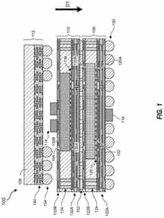
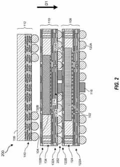
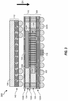
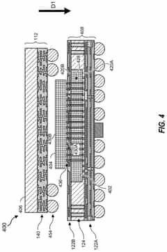
3D chiplet integration using fan-out wafer-level packaging
PatentPendingUS20240274587A1
Innovation
- The use of fan-out wafer-level packaging and three-dimensional packaging techniques for combining semiconductor chips and embedded memory in configurations such as face-to-back, back-to-back, and face-to-face orientations, enabling direct connections between chiplets and reducing assembly package sizes and manufacturing complexity.
Supply Chain Security for Chiplets
PatentPendingUS20250155500A1
Innovation
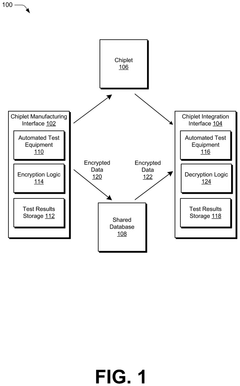
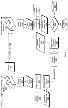
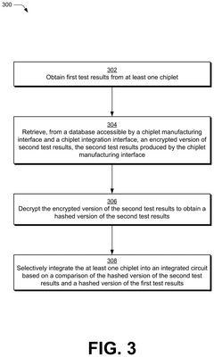
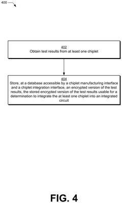
- A system is implemented where a chiplet manufacturing interface tests each chiplet, records the test results securely, and encrypts them using a public-private key pair. These encrypted test results are stored in a shared database accessible by the chiplet integration interface, which decrypts and compares them with its own test results to verify the chiplet's trustworthiness before integration.
Regulatory Framework Impact on Chiplet Development
The regulatory landscape surrounding chiplet technology is evolving rapidly as governments and international bodies recognize the strategic importance of semiconductor innovation. Current regulatory frameworks primarily focus on traditional monolithic chip designs, creating a significant gap in addressing the unique characteristics of chiplet integration. This regulatory uncertainty poses challenges for companies investing in chiplet technology, as compliance requirements remain unclear across different jurisdictions.
Export control regulations, particularly those implemented by the United States, European Union, and China, have direct implications for chiplet development. These regulations restrict the transfer of advanced semiconductor technologies to certain countries, potentially limiting global collaboration in chiplet innovation. Companies must navigate complex compliance requirements when sharing chiplet designs or manufacturing processes across international boundaries, which can slow development cycles and increase costs.
Intellectual property protection represents another critical regulatory challenge for chiplet integration. The modular nature of chiplets, where components from different vendors are integrated into a single package, creates complex IP ownership scenarios. Current patent frameworks may not adequately address the collaborative nature of chiplet design, leading to potential disputes over IP rights and licensing terms. This regulatory uncertainty can discourage companies from fully embracing chiplet technology.
Data security and privacy regulations also impact chiplet development, particularly for applications in sensitive sectors like healthcare, finance, and defense. Chiplet-based systems must comply with regulations such as GDPR in Europe or CCPA in California when processing personal data. The distributed nature of chiplet manufacturing may create additional compliance challenges when components are sourced from multiple jurisdictions with varying data protection standards.
Standardization efforts are emerging as a regulatory response to chiplet integration challenges. Organizations like JEDEC, IEEE, and the Open Compute Project are developing technical standards for chiplet interfaces and packaging. These industry-led initiatives aim to create a more predictable regulatory environment while ensuring interoperability between chiplets from different vendors. However, the voluntary nature of these standards means their effectiveness depends on widespread industry adoption.
Environmental regulations increasingly influence chiplet development, with requirements for energy efficiency, material usage, and end-of-life recycling. The European Union's Eco-design Directive and Restriction of Hazardous Substances (RoHS) regulations set specific parameters that chiplet manufacturers must meet. While chiplets potentially offer environmental benefits through more efficient resource utilization, demonstrating compliance with these regulations requires additional testing and documentation.
Cross-Border Technology Transfer Considerations
The global nature of semiconductor supply chains and the strategic importance of chiplet technology have created a complex landscape for cross-border technology transfers. As nations increasingly view advanced semiconductor capabilities as critical to national security, chiplet integration technologies face heightened scrutiny under export control regimes. Companies developing modular chip solutions must navigate a fragmented regulatory environment where different countries impose varying restrictions on semiconductor IP, manufacturing equipment, and design tools.
The United States has implemented significant export controls targeting advanced semiconductor technologies, particularly those with potential military applications. These regulations directly impact chiplet integration by restricting access to cutting-edge packaging technologies and manufacturing equipment. Similarly, the European Union has established its own framework for controlling strategic technology transfers, while maintaining a commitment to open research collaboration within defined parameters.
Asian technology hubs present a particularly nuanced regulatory landscape. Japan and South Korea have aligned closely with Western regulatory approaches while maintaining robust semiconductor ecosystems. China's push for semiconductor self-sufficiency has prompted increased scrutiny of technology transfers involving chiplet integration, creating challenges for multinational R&D collaborations and supply chain integration.
Intellectual property protection represents another critical dimension of cross-border technology transfer. Chiplet designs often incorporate IP from multiple sources across different jurisdictions, requiring careful management of licensing agreements and compliance with varying IP protection standards. Companies must implement robust protocols to prevent unauthorized technology transfers while maintaining necessary collaboration with global partners.
The standardization of chiplet interfaces presents both challenges and opportunities for cross-border technology transfer. While open standards like Universal Chiplet Interconnect Express (UCIe) facilitate global collaboration, they also raise questions about technology control and competitive advantage. Regulatory frameworks must balance innovation promotion with strategic technology protection.
Looking forward, companies engaged in chiplet integration must develop comprehensive compliance strategies that address the evolving regulatory landscape. This includes conducting thorough due diligence on international partners, implementing strong IP protection measures, and maintaining visibility across global supply chains. Regulatory expertise has become as essential as technical knowledge in successfully deploying chiplet integration technologies across international boundaries.
Unlock deeper insights with PatSnap Eureka Quick Research — get a full tech report to explore trends and direct your research. Try now!
Generate Your Research Report Instantly with AI Agent
Supercharge your innovation with PatSnap Eureka AI Agent Platform!