

Chiplet Integration's Impact on Modern Semiconductor Processes
OCT 15, 20259 MIN READ
Generate Your Research Report Instantly with AI Agent
Patsnap Eureka helps you evaluate technical feasibility & market potential.
Chiplet Technology Evolution and Objectives
The evolution of semiconductor technology has been characterized by a relentless pursuit of performance improvements through transistor scaling, following Moore's Law for decades. However, as traditional scaling approaches physical limitations around the 7nm node and below, the industry has been forced to explore alternative approaches to maintain performance trajectory. Chiplet technology emerged as a revolutionary paradigm shift, enabling the disaggregation of monolithic system-on-chip (SoC) designs into smaller functional blocks that can be manufactured separately and then integrated.
The concept of chiplets dates back to the early 2000s, but gained significant momentum around 2017 when major semiconductor companies began implementing commercial solutions. AMD's introduction of their "Infinity Fabric" interconnect technology with the Zen microarchitecture marked a pivotal moment, demonstrating that high-performance computing products could be successfully built using a chiplet-based approach. Intel followed with their EMIB (Embedded Multi-die Interconnect Bridge) and later Foveros technologies, while TSMC developed their InFO (Integrated Fan-Out) and CoWoS (Chip on Wafer on Substrate) packaging platforms.
The primary objective of chiplet technology is to overcome the economic and technical challenges associated with monolithic integration at advanced nodes. By partitioning complex designs into smaller dies, manufacturers can optimize yield, reduce costs, and enable heterogeneous integration of components fabricated using different process technologies. This approach allows critical components requiring cutting-edge performance to be manufactured at the most advanced nodes, while less demanding components can utilize more mature, cost-effective processes.
Another key objective is to enable more flexible product development strategies. The modular nature of chiplets allows companies to mix and match different functional blocks, creating diverse product offerings from a common set of building blocks. This significantly reduces time-to-market for new products and enables more efficient resource allocation in the development process.
Looking forward, the industry aims to establish standardized chiplet interfaces and protocols to create a more open ecosystem. Initiatives like the Universal Chiplet Interconnect Express (UCIe) consortium are working toward creating industry standards that would allow chiplets from different vendors to be seamlessly integrated. This "chiplet marketplace" concept could fundamentally transform semiconductor business models, enabling smaller companies to focus on specialized chiplet designs without needing to develop complete SoC solutions.
The ultimate technical goal is to achieve "chiplet integration" that approaches or matches the performance, power efficiency, and reliability of monolithic designs while offering superior economics and flexibility. This requires continuous innovation in packaging technologies, interconnect solutions, and design methodologies to minimize the overhead associated with die-to-die communication.
Market Demand Analysis for Chiplet Solutions
The global semiconductor market is experiencing a paradigm shift towards chiplet-based architectures, driven by increasing demand for higher performance, improved power efficiency, and cost-effective scaling. Market research indicates that the chiplet solutions market is projected to grow at a compound annual growth rate of over 40% from 2023 to 2030, reaching approximately $50 billion by the end of the decade. This explosive growth reflects the industry's recognition of chiplets as a viable solution to the limitations of traditional monolithic chip designs.
Consumer electronics, particularly smartphones, tablets, and laptops, represent the largest market segment for chiplet solutions, accounting for roughly 35% of the total demand. These devices require increasingly powerful processors while maintaining energy efficiency and form factor constraints that chiplets can effectively address. The high-performance computing sector follows closely, with data centers and cloud service providers actively adopting chiplet architectures to meet the computational demands of artificial intelligence and machine learning workloads.
Automotive applications represent the fastest-growing segment for chiplet technology, with an estimated growth rate exceeding 50% annually. Advanced driver-assistance systems (ADAS), autonomous driving capabilities, and in-vehicle infotainment systems all benefit from the performance and integration advantages that chiplet designs offer. The automotive industry's stringent reliability requirements and extended product lifecycles also align well with the modular nature of chiplets, allowing for more targeted component updates.
The telecommunications sector, particularly with the ongoing global 5G infrastructure deployment, has emerged as another significant market for chiplet solutions. Network equipment manufacturers are leveraging chiplet designs to create more efficient and scalable base stations and network processing units. Industry analysts estimate that approximately 25% of 5G infrastructure equipment will incorporate chiplet technology by 2025.
Geographically, North America currently leads the chiplet solutions market with approximately 40% market share, followed by Asia-Pacific at 35% and Europe at 20%. However, the Asia-Pacific region is expected to demonstrate the highest growth rate over the next five years due to substantial investments in semiconductor manufacturing capabilities in countries like Taiwan, South Korea, and China.
Supply chain considerations are increasingly influencing market demand patterns. The recent global semiconductor shortage has highlighted the strategic importance of flexible manufacturing approaches, with chiplet designs offering advantages in production yield and resource utilization. Major foundries report that chiplet-based designs can improve manufacturing yields by 15-30% compared to equivalent monolithic designs, translating to significant cost savings and improved product availability.
Current Chiplet Integration Challenges
Despite the promising advancements in chiplet technology, significant integration challenges persist that impede its widespread adoption. The primary challenge lies in the interconnection between chiplets, where traditional package-level connections struggle to match the bandwidth, latency, and power efficiency of monolithic designs. Current die-to-die interfaces such as Intel's EMIB, TSMC's CoWoS, and AMD's Infinity Fabric each present trade-offs between performance, manufacturing complexity, and cost that must be carefully balanced.
Thermal management represents another critical obstacle, as heterogeneous integration of chiplets with different power densities creates hotspots and thermal gradients that can compromise system reliability. The industry has yet to develop standardized solutions for efficient heat dissipation across multiple dies with varying thermal characteristics, particularly in high-performance computing applications where power densities continue to increase.
Testing and yield management introduce additional complexities in the chiplet paradigm. Known-good-die testing becomes essential but remains challenging to implement comprehensively, as some failure modes only manifest when chiplets interact within the complete system. This creates a testing paradox where full functionality verification requires complete assembly, yet assembly should ideally only proceed with verified components.
Design and verification methodologies for chiplet-based systems lack maturity compared to traditional SoC approaches. Current EDA tools were primarily developed for monolithic designs and require significant adaptation to effectively model multi-die interactions, signal integrity across interfaces, and power distribution networks spanning multiple chiplets. The industry faces a toolchain gap that slows design cycles and increases engineering costs.
Standardization remains perhaps the most pressing industry-wide challenge. Despite efforts from consortia like UCIe (Universal Chiplet Interconnect Express), the ecosystem still lacks widely adopted standards for chiplet interfaces, protocols, and physical specifications. This fragmentation inhibits the development of a truly open chiplet marketplace where components from different vendors can be seamlessly integrated.
Manufacturing alignment presents practical hurdles as well, with different chiplets potentially requiring different process nodes, packaging technologies, and manufacturing partners. Coordinating supply chains across these variables introduces logistical complexities that can impact time-to-market and overall system costs, particularly for smaller companies with limited manufacturing leverage.
Current Chiplet Integration Methodologies
01 Performance and Efficiency Improvements in Chiplet Integration
Chiplet integration enables significant performance and efficiency improvements in semiconductor devices. By breaking down complex systems into smaller, specialized chiplets, manufacturers can optimize each component separately, leading to better overall system performance. This approach allows for more efficient power management, reduced thermal issues, and improved processing capabilities. The modular nature of chiplets also enables heterogeneous integration of different process technologies, further enhancing performance while maintaining power efficiency.- Performance and Efficiency Improvements: Chiplet integration enables significant performance and efficiency improvements in semiconductor devices. By breaking down complex systems into smaller, specialized chiplets, manufacturers can optimize each component for specific functions. This modular approach allows for better thermal management, reduced power consumption, and enhanced processing capabilities. The integration of heterogeneous chiplets with different process technologies can deliver superior performance compared to monolithic designs while maintaining cost-effectiveness.
- Advanced Packaging Technologies: Chiplet integration relies on advanced packaging technologies to connect multiple dies efficiently. These technologies include interposers, through-silicon vias (TSVs), and advanced substrate materials that facilitate high-bandwidth, low-latency communication between chiplets. The packaging solutions address challenges related to signal integrity, power delivery, and thermal management while enabling higher integration density. These advanced packaging approaches are crucial for realizing the full potential of chiplet-based designs in modern computing systems.
- Manufacturing and Cost Implications: Chiplet integration offers significant manufacturing advantages and cost benefits. By using smaller dies, manufacturers can achieve higher yield rates compared to large monolithic designs, as defects impact smaller areas of silicon. This approach allows for more efficient use of wafer area and enables mixing of different process nodes, optimizing cost-performance trade-offs. Additionally, chiplet designs provide flexibility in component selection and facilitate easier updates to specific functions without redesigning the entire system.
- System-Level Integration Challenges: Chiplet integration presents unique system-level challenges that impact overall design and implementation. These include managing communication protocols between chiplets, addressing latency issues in inter-chiplet connections, ensuring power integrity across the system, and developing standardized interfaces. The complexity of testing integrated chiplet systems also increases, requiring new methodologies for validation. Overcoming these challenges requires innovative design approaches and collaboration across the semiconductor ecosystem.
- Emerging Applications and Future Trends: Chiplet integration is enabling new applications across various domains including artificial intelligence, high-performance computing, and edge devices. The technology allows for customized solutions that combine specialized accelerators, memory systems, and processing elements tailored to specific workloads. Future trends include increased standardization of chiplet interfaces, development of chiplet marketplaces, and integration with advanced technologies such as photonics and new memory architectures, potentially revolutionizing semiconductor design and manufacturing approaches.
02 Manufacturing and Packaging Innovations for Chiplet Technology
Advanced manufacturing and packaging technologies are crucial for successful chiplet integration. These innovations include new interconnect methods, die-to-die bonding techniques, and advanced substrate technologies that enable high-bandwidth, low-latency communication between chiplets. Three-dimensional integration approaches allow for vertical stacking of chiplets, maximizing silicon utilization while minimizing footprint. Novel packaging solutions address thermal management challenges and improve signal integrity between the integrated components.Expand Specific Solutions03 System Architecture and Design Considerations for Chiplet-Based Solutions
Chiplet integration introduces new system architecture paradigms that require careful design considerations. This includes developing standardized interfaces between chiplets, implementing efficient data routing protocols, and creating coherent memory systems across multiple dies. System designers must address challenges related to clock distribution, power delivery, and thermal management across chiplet boundaries. The architecture must also support flexible configurations to accommodate different application requirements while maintaining system reliability and performance.Expand Specific Solutions04 Economic and Supply Chain Implications of Chiplet Technology
Chiplet integration has significant economic and supply chain implications for the semiconductor industry. By enabling the reuse of proven IP blocks and allowing for mix-and-match of components from different process nodes, chiplet technology can reduce development costs and time-to-market. This approach also improves manufacturing yield by limiting the size of individual dies. Additionally, chiplet technology enables more flexible supply chain strategies, allowing companies to source different components from specialized manufacturers and potentially reducing dependency on single suppliers.Expand Specific Solutions05 Future Trends and Applications of Chiplet Integration
Emerging trends in chiplet integration point toward increasingly sophisticated applications across various domains. Future developments include enhanced AI and machine learning capabilities through specialized accelerator chiplets, improved edge computing solutions with customizable chiplet configurations, and advanced networking systems with integrated high-speed communication chiplets. The technology is also enabling new possibilities in automotive electronics, medical devices, and other specialized applications where customization, reliability, and performance are critical requirements.Expand Specific Solutions
Key Industry Players in Chiplet Ecosystem
Chiplet integration is transforming semiconductor manufacturing by enabling modular chip design, currently in its growth phase with significant market expansion anticipated. The technology has reached moderate maturity, with industry leaders like TSMC, Intel, and AMD driving innovation through advanced packaging solutions. Samsung, Qualcomm, and IBM are investing heavily in heterogeneous integration techniques, while SMIC and Micron focus on memory-logic integration. Academic institutions including Tsinghua University and Fudan University collaborate with industry on research initiatives. The market is characterized by strategic partnerships between foundries and design houses, with competition intensifying as companies seek to establish technical standards and ecosystem dominance in this rapidly evolving space.
Taiwan Semiconductor Manufacturing Co., Ltd.
Technical Solution: TSMC has developed comprehensive chiplet integration technologies through its 3DFabric platform, which encompasses both frontend and backend integration solutions. Their System on Integrated Chips (SoIC) technology enables ultra-high-density interconnects between chiplets with pitches as small as 9 micrometers, significantly outperforming traditional packaging methods[7]. TSMC's Chip-on-Wafer-on-Substrate (CoWoS) technology combines multiple chiplets on a silicon interposer, providing high-bandwidth, low-power connections between heterogeneous dies. This has been crucial for AI accelerators and high-performance computing applications, with recent iterations supporting up to 12 HBM memory stacks alongside compute chiplets[8]. Their Integrated Fan-Out (InFO) technology offers a lower-cost alternative for less demanding applications, eliminating the need for an interposer while still enabling multi-chiplet integration. TSMC has also developed their 3D Stacking SoIC technology, which allows for direct wafer-to-wafer bonding with extremely fine pitch connections, enabling true 3D integration of logic chiplets[9].
Strengths: TSMC offers the most comprehensive suite of chiplet integration technologies spanning different price/performance points, and their position as the leading foundry gives them unparalleled process integration capabilities across nodes. Weaknesses: As a pure-play foundry, TSMC depends on customers and partners for chiplet designs and standards, potentially limiting their ability to drive architectural innovation compared to IDMs like Intel.
Advanced Micro Devices, Inc.
Technical Solution: AMD revolutionized chiplet architecture with its Infinity Fabric interconnect technology, first commercially deployed at scale in its Ryzen and EPYC processors. Their chiplet approach disaggregates CPU cores from I/O functions, allowing optimal manufacturing processes for each component. The core chiplets (CCDs) are manufactured on advanced nodes (e.g., TSMC 5nm) for maximum performance and efficiency, while I/O dies use mature processes (e.g., 12nm) for cost optimization and better analog circuit performance[4]. AMD's 3rd Gen EPYC server processors feature up to 9 chiplets (8 core chiplets plus one I/O die) in a single package, demonstrating the scalability of their approach. Their Infinity Fabric provides coherent communication between chiplets with high bandwidth (up to 36GB/s per link) and low latency[5]. AMD has continued evolving this architecture with their latest Zen 4 processors, incorporating 3D V-Cache technology that stacks additional cache memory directly on top of compute chiplets, further demonstrating the flexibility of chiplet integration[6].
Strengths: AMD's approach enables cost-effective scaling of core counts and optimizes manufacturing yield by using smaller chiplets. Their implementation has proven commercially successful across consumer and enterprise markets. Weaknesses: The disaggregated design introduces some latency overhead between chiplets compared to monolithic designs, and their interconnect technology has been primarily optimized for their own products rather than as a universal standard for the industry.
Critical Patents and Technical Innovations
Chiplet arrangement
PatentActiveEP4451135A1
Innovation
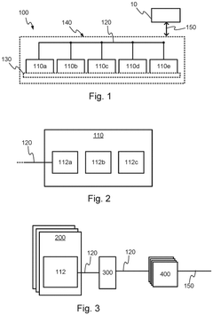
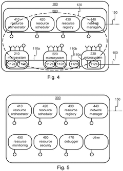
- A chiplet arrangement with a control plane that orchestrates microsystems and microservices, allowing for dynamic instantiation based on hardware resource availability and utilization, featuring a resource orchestrator, network manager, and resource scheduler to optimize resource utilization, scalability, and power management.
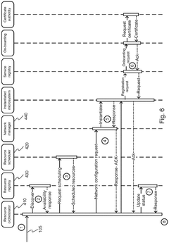
Technologies for a unified test and debug architecture
PatentWO2024205614A1
Innovation
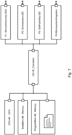
- A unified test and debug architecture is implemented using an external hardware debug interface that is interface-agnostic, employing Universal Chiplet Interconnect Express (UCIe) packets for debug messages, allowing for seamless communication and interoperability between chiplets, and enabling testing at various stages from sort stage to infield debugging.

Supply Chain Implications for Chiplet Manufacturing
The shift towards chiplet architecture has fundamentally transformed semiconductor supply chains, creating both opportunities and challenges for manufacturers. Traditional monolithic chip production relied on vertically integrated supply chains where a single manufacturer controlled most processes. Chiplet manufacturing, however, introduces a more distributed model where different companies can specialize in producing specific chiplets that are later integrated into a complete system.
This fragmentation enables smaller players to enter the market by focusing on niche chiplet designs rather than investing in complete chip manufacturing capabilities. Companies can leverage their specific expertise in areas such as memory, I/O, or specialized processing units without bearing the full burden of advanced node manufacturing costs. This specialization has created new tiers of suppliers within the semiconductor ecosystem.
Inventory management becomes more complex in chiplet-based manufacturing. While traditional monolithic chips represent single inventory units, chiplet-based systems require coordinating multiple components with different lead times and yield rates. This complexity necessitates more sophisticated supply chain management systems and closer coordination between partners to ensure all necessary chiplets are available for final integration.
Testing and quality assurance processes also face significant changes. Each chiplet must be individually tested before integration, and additional testing is required after assembly to verify inter-chiplet communications. This multi-stage testing increases supply chain complexity but potentially improves overall yields by allowing defective chiplets to be identified and removed before final assembly.
Geopolitical considerations have gained prominence as chiplet manufacturing distributes production across multiple regions. Supply chain resilience strategies now include geographic diversification of chiplet suppliers to mitigate regional disruptions. However, this distribution also introduces new challenges in maintaining consistent manufacturing standards and intellectual property protection across different jurisdictions.
The chiplet approach has accelerated the adoption of advanced packaging technologies throughout the supply chain. Manufacturers must now develop or source capabilities in areas such as silicon interposers, through-silicon vias (TSVs), and micro-bump technologies. This has created new specialized segments within the semiconductor supply chain focused exclusively on advanced packaging and integration services.
Standardization efforts are emerging as critical factors in supply chain efficiency. Industry consortia are working to establish common interfaces and protocols for chiplet integration, which would enable more flexible sourcing strategies and reduce dependency on proprietary integration technologies. These standards will be essential for realizing the full supply chain benefits of the chiplet approach.
Standardization Efforts in Chiplet Interfaces
The standardization of chiplet interfaces represents a critical evolutionary step in the semiconductor industry's transition toward disaggregated chip designs. As chiplet technology gains momentum, the lack of universal standards has emerged as a significant barrier to widespread adoption. Several industry consortia have formed to address this challenge, with the Universal Chiplet Interconnect Express (UCIe) consortium leading efforts since 2022. This alliance, which includes major players like Intel, AMD, Arm, TSMC, and Samsung, aims to establish open specifications for die-to-die interconnection.
UCIe focuses on standardizing both the physical and protocol layers of chiplet interfaces, enabling seamless integration of chiplets from different vendors. The standard encompasses multiple aspects including electrical signaling, physical design parameters, and communication protocols that facilitate high-bandwidth, low-latency connections between chiplets.
Parallel to UCIe, other notable standardization initiatives include JEDEC's development of the Chiplet Physical Interface (CXL) standard and the Open Domain-Specific Architecture (ODSA) group's Bunch of Wires (BoW) specification. These complementary efforts address different aspects of the chiplet ecosystem, from high-performance computing applications to cost-effective implementations for various market segments.
The Advanced Interface Bus (AIB) developed by Intel represents another significant contribution to standardization efforts. Recently released as an open standard, AIB provides specifications for die-to-die connections that balance performance, power efficiency, and implementation complexity.
Standardization efforts face several technical challenges, including managing signal integrity across chiplet boundaries, addressing thermal considerations in densely packed multi-chiplet designs, and ensuring backward compatibility with existing systems. The trade-off between performance optimization and universal compatibility remains a central tension in the development of these standards.
The economic implications of successful standardization are substantial. Industry analysts project that standardized interfaces could reduce design costs by 20-30% while accelerating time-to-market by similar margins. Furthermore, standardization enables a more diverse ecosystem where specialized manufacturers can focus on their core competencies, potentially reshaping the semiconductor value chain.
Looking forward, the evolution of these standards will likely follow a path similar to other successful technology standards, with initial fragmentation followed by convergence around dominant approaches. The industry's ability to establish and widely adopt these standards will significantly influence the pace at which chiplet-based architectures transform semiconductor manufacturing processes.
Unlock deeper insights with Patsnap Eureka Quick Research — get a full tech report to explore trends and direct your research. Try now!
Generate Your Research Report Instantly with AI Agent
Supercharge your innovation with Patsnap Eureka AI Agent Platform!