Chiplet Integration and Its Role in Semiconductor Innovations
OCT 15, 20259 MIN READ
Generate Your Research Report Instantly with AI Agent
Patsnap Eureka helps you evaluate technical feasibility & market potential.
Chiplet Technology Evolution and Objectives
The concept of chiplets emerged as a response to the growing challenges in traditional monolithic semiconductor design. As Moore's Law faced physical limitations, the industry began exploring alternative approaches to continue performance scaling. Chiplets represent a paradigm shift from single-die integration to a more modular approach, where multiple smaller dies are integrated into a single package.
The evolution of chiplet technology can be traced back to the early 2010s when companies like AMD began experimenting with multi-chip modules. The introduction of AMD's Zen architecture in 2017 marked a significant milestone, demonstrating the commercial viability of chiplet-based designs. This approach allowed for better yield management and cost optimization compared to large monolithic dies.
Intel followed with its Embedded Multi-die Interconnect Bridge (EMIB) technology, while TSMC developed its Integrated Fan-Out (InFO) and Chip-on-Wafer-on-Substrate (CoWoS) packaging technologies. These developments signaled the industry's growing commitment to heterogeneous integration as a strategic direction for semiconductor advancement.
The primary objective of chiplet technology is to overcome the limitations of traditional semiconductor scaling. By disaggregating complex SoCs into smaller functional blocks, manufacturers can optimize each component using the most appropriate process node. This approach enables continued performance improvements while managing costs and manufacturing complexity.
Another key objective is to enhance design flexibility and reusability. Chiplets allow companies to mix and match pre-validated IP blocks, potentially reducing development time and risks. This modular approach also facilitates heterogeneous integration, combining components from different process nodes or even different materials within a single package.
Looking forward, the industry aims to establish standardized interfaces for chiplet integration. Initiatives like the Universal Chiplet Interconnect Express (UCIe) consortium are working to create open specifications that would enable interoperability between chiplets from different vendors. This standardization represents a crucial step toward creating a more diverse and competitive chiplet ecosystem.
The long-term vision for chiplet technology extends beyond traditional computing applications. As domains like artificial intelligence, edge computing, and IoT continue to grow, chiplet-based designs offer the flexibility to create highly specialized, application-specific solutions while maintaining manufacturing efficiency. The ability to integrate diverse technologies—from digital logic to memory, analog, and RF components—positions chiplets as a foundational technology for next-generation semiconductor innovations.
Market Demand Analysis for Chiplet Solutions
The global semiconductor market is experiencing a paradigm shift towards chiplet-based architectures, driven by increasing demand for higher performance, improved power efficiency, and cost-effective scaling. Market analysis indicates that the traditional monolithic chip design approach is reaching physical and economic limitations, creating substantial market opportunities for chiplet solutions. According to industry reports, the chiplet market is projected to grow at a compound annual growth rate of over 40% from 2023 to 2030, potentially reaching tens of billions of dollars by the end of the decade.
This remarkable growth is primarily fueled by data centers and high-performance computing sectors, which require increasingly powerful processors to handle artificial intelligence, machine learning, and big data applications. These applications demand computational capabilities that are becoming increasingly difficult to achieve through traditional semiconductor scaling approaches. The hyperscaler companies like Google, Amazon, and Microsoft are actively investing in chiplet-based solutions to address their exponentially growing computational needs.
Consumer electronics represents another significant market segment driving chiplet adoption. Smartphone manufacturers, PC makers, and gaming console producers are exploring chiplet architectures to deliver enhanced performance while managing thermal constraints and power consumption. The automotive industry is also emerging as a key market for chiplet technology, particularly with the rise of autonomous driving systems requiring sophisticated computing platforms.
From a geographical perspective, North America currently leads the chiplet market due to the presence of major semiconductor companies and technology giants. However, Asia-Pacific is expected to witness the fastest growth, with significant investments in semiconductor manufacturing and design capabilities in countries like Taiwan, South Korea, and China.
The market demand for chiplet solutions is further accelerated by supply chain considerations. The semiconductor industry has faced unprecedented challenges in recent years, including chip shortages and geopolitical tensions affecting global supply chains. Chiplet architecture offers greater manufacturing flexibility and potentially better yield management, which is particularly valuable in the current market environment.
Industry surveys indicate that over 70% of semiconductor companies are now investing in chiplet-related technologies, recognizing it as a strategic direction for future product development. This widespread industry adoption signals strong market confidence in chiplet solutions as a fundamental approach to addressing the technical and economic challenges facing the semiconductor industry in the post-Moore's Law era.
Current Chiplet Integration Challenges
Despite the promising advancements in chiplet technology, significant technical challenges persist in achieving seamless integration. The primary obstacle remains the development of high-bandwidth, low-latency, and energy-efficient die-to-die interconnects. Current solutions like Intel's EMIB, TSMC's SoIC, and AMD's Infinity Fabric each present trade-offs between performance, power consumption, and manufacturing complexity that have not been fully optimized.
Thermal management presents another critical challenge as heterogeneous integration creates uneven heat distribution across the package. Hotspots can form at interconnect junctions, potentially compromising system reliability and performance. Traditional cooling solutions designed for monolithic chips often prove inadequate for the complex thermal profiles of chiplet-based designs.
Testing methodologies for chiplet-based systems remain underdeveloped. The industry lacks standardized approaches for known-good-die testing before integration, resulting in yield challenges that can offset the cost advantages of chiplet architectures. Post-integration testing is further complicated by limited access to internal interconnects, making fault isolation and diagnosis particularly difficult.
Design and verification tools present significant barriers to widespread chiplet adoption. Current EDA platforms were primarily developed for monolithic chip design and lack robust support for multi-die systems. Designers struggle with modeling the complex interactions between chiplets, particularly when integrating components from different vendors with varying process technologies.
The absence of universal standards for chiplet interfaces represents perhaps the most significant industry-wide challenge. While initiatives like UCIe (Universal Chiplet Interconnect Express) show promise, the ecosystem remains fragmented. This fragmentation impedes the development of a true chiplet marketplace where components from different vendors could be seamlessly integrated, limiting the technology's potential for democratizing semiconductor innovation.
Manufacturing challenges persist in achieving precise alignment during assembly. Advanced packaging techniques require positioning accuracy measured in microns, with even minor misalignments potentially causing catastrophic connection failures. Current equipment capabilities struggle to meet these precision requirements at high throughput rates necessary for volume production.
Supply chain complexity increases substantially with chiplet designs. Coordinating multiple fabrication processes, potentially across different foundries, introduces logistical challenges and dependencies that can impact time-to-market and resilience to supply disruptions. This complexity is particularly challenging for smaller companies with limited resources and supplier relationships.
Current Chiplet Integration Methodologies
01 Interconnect technologies for chiplet integration
Various interconnect technologies are employed to facilitate communication between chiplets in multi-die systems. These include advanced packaging techniques, silicon interposers, and bridge technologies that enable high-bandwidth, low-latency connections between different chiplets. The interconnect architecture is crucial for maintaining performance while allowing modular design approaches, with technologies such as through-silicon vias (TSVs) and micro-bumps enabling vertical stacking and horizontal integration of chiplets.- Interconnect technologies for chiplet integration: Various interconnect technologies are employed to enable efficient communication between chiplets in multi-die systems. These include advanced packaging techniques, high-bandwidth interfaces, and specialized interconnect fabrics that facilitate die-to-die communication. These technologies aim to minimize latency, maximize bandwidth, and ensure reliable data transfer between integrated chiplets, which is crucial for maintaining system performance in disaggregated chip architectures.
- Thermal management solutions for chiplet designs: Thermal management is critical in chiplet integration due to the high power density and heat generation in multi-die packages. Solutions include advanced cooling techniques, thermal interface materials, and strategic placement of chiplets to optimize heat dissipation. Effective thermal management prevents performance degradation, ensures reliability, and extends the lifespan of chiplet-based systems by maintaining optimal operating temperatures across all integrated components.
- Power delivery architectures for chiplet systems: Specialized power delivery architectures are designed to meet the unique requirements of chiplet-based systems. These include distributed power delivery networks, integrated voltage regulators, and power management techniques that optimize energy efficiency across multiple dies. Effective power delivery is essential for maintaining stable operation, minimizing power loss, and supporting the varying power requirements of different chiplets within an integrated system.
- Testing and validation methodologies for chiplet integration: Comprehensive testing and validation methodologies are developed specifically for chiplet-based designs to ensure functionality, performance, and reliability. These include pre-integration testing of individual chiplets, interface validation, system-level testing, and specialized techniques for identifying integration issues. Advanced testing approaches help maintain quality control, improve yield rates, and ensure that chiplet-based systems meet performance specifications and reliability requirements.
- Heterogeneous integration of chiplets with different process technologies: Heterogeneous integration enables combining chiplets manufactured using different process technologies, materials, or from different vendors into a single package. This approach allows for optimizing each component for its specific function while maintaining system-level integration. Benefits include improved performance, reduced costs, enhanced functionality, and the ability to combine specialized components such as memory, processors, and analog circuits in novel configurations that would be impossible in monolithic designs.
02 Thermal management in chiplet designs
Thermal management is a critical consideration in chiplet integration due to the high power density and heat generation in tightly packed multi-die systems. Solutions include specialized thermal interface materials, integrated heat spreaders, and advanced cooling techniques designed specifically for chiplet architectures. Effective thermal management strategies help maintain optimal operating temperatures across all chiplets, preventing performance degradation and ensuring reliability in high-performance computing applications.Expand Specific Solutions03 Power delivery and distribution for chiplet systems
Power delivery networks for chiplet-based designs require specialized approaches to ensure stable voltage and current distribution across multiple dies. This includes innovative power delivery architectures, integrated voltage regulators, and power management techniques that address the unique challenges of supplying power to heterogeneous chiplet configurations. Efficient power distribution is essential for maintaining performance while minimizing power consumption in complex chiplet-based systems.Expand Specific Solutions04 Testing and yield optimization for chiplet-based systems
Testing methodologies for chiplet-based systems involve both pre-integration testing of individual chiplets and post-integration system-level testing. Known-good-die testing, built-in self-test capabilities, and specialized test interfaces are employed to ensure functionality and performance. Yield optimization strategies leverage the modular nature of chiplet designs, allowing manufacturers to mix and match tested chiplets to achieve higher overall system yields compared to monolithic designs.Expand Specific Solutions05 Heterogeneous integration of chiplets
Heterogeneous integration involves combining chiplets manufactured using different process technologies or containing different functional blocks into a single package. This approach allows optimization of each chiplet for its specific function, combining high-performance logic, memory, analog/RF, and other specialized components. Advanced packaging technologies enable the integration of these diverse chiplets while maintaining high-bandwidth, low-latency communication between them, resulting in systems with optimized performance, power efficiency, and cost.Expand Specific Solutions
Leading Semiconductor Companies in Chiplet Space
The chiplet integration market is experiencing rapid growth as the semiconductor industry transitions from traditional monolithic designs to modular approaches. Currently in an early growth phase, this technology is gaining momentum with a projected market size exceeding $50 billion by 2030. Leading players like TSMC, Intel, and AMD are at the forefront, with TSMC's advanced packaging technologies setting industry standards. Samsung and SK hynix are making significant investments, while IBM and Micron focus on memory-centric chiplet solutions. Chinese companies including SMIC are developing domestic capabilities to reduce dependency on foreign technologies. The ecosystem is maturing with standardization efforts, though challenges in interconnect technologies and thermal management remain.
Taiwan Semiconductor Manufacturing Co., Ltd.
Technical Solution: TSMC has developed a comprehensive chiplet integration platform called 3DFabric, which encompasses multiple technologies for chip integration. Their Chip-on-Wafer-on-Substrate (CoWoS) technology uses silicon interposers to connect multiple chiplets with thousands of interconnections, providing significantly higher bandwidth than traditional packaging methods. TSMC's Integrated Fan-Out (InFO) technology offers a less expensive alternative for applications that don't require the extreme interconnect density of CoWoS. Their System-on-Integrated-Chips (SoIC) technology enables true 3D stacking with microbump-free hybrid bonding, achieving sub-10 micron pitches and extremely high interconnect density. TSMC has demonstrated these technologies in various customer products, including high-performance computing chips that combine HBM memory with processing cores on a single package. Their advanced packaging technologies support heterogeneous integration of chips manufactured on different process nodes, enabling customers to optimize performance, power, and cost.
Strengths: TSMC offers the most advanced and diverse range of chiplet integration technologies in the industry, with proven high-volume manufacturing capabilities. Their position as the leading semiconductor foundry gives them unique insights into integration requirements across multiple market segments. Weaknesses: Their advanced packaging solutions, particularly CoWoS, can be expensive and face capacity constraints due to high demand, and some technologies require significant design expertise to implement effectively.
Samsung Electronics Co., Ltd.
Technical Solution: Samsung's chiplet integration strategy centers around their advanced packaging technologies, particularly their X-Cube (eXtended-Cube) technology that enables high-bandwidth, low-power 3D integration of heterogeneous chiplets. This technology utilizes through-silicon vias (TSVs) and microbumps to create vertical electrical connections between stacked dies. Samsung has demonstrated this capability in memory-centric applications, stacking HBM (High Bandwidth Memory) with logic processors to dramatically reduce the physical distance between memory and compute resources. Their I-Cube (Interposer-Cube) technology uses silicon interposers to connect multiple chiplets horizontally with high-density interconnects. Samsung has also developed hybrid bonding techniques that enable direct copper-to-copper connections between dies without microbumps, achieving interconnect pitches below 10 microns. In their memory business, Samsung has leveraged chiplet concepts to develop their HBM-PIM (Processing-In-Memory) architecture, which integrates computational elements directly within memory stacks to address data movement bottlenecks in AI applications. Their comprehensive semiconductor ecosystem, spanning memory, logic, and foundry services, positions them uniquely to explore diverse chiplet integration approaches.
Strengths: Samsung's vertical integration across memory, logic design, and manufacturing enables them to optimize complete chiplet-based systems. Their memory expertise gives them advantages in developing high-bandwidth die-to-die interconnects. Weaknesses: Samsung has been somewhat less public about their chiplet roadmap compared to competitors, and their foundry business faces challenges in competing with TSMC's advanced packaging ecosystem.
Key Patents and Research in Chiplet Technology
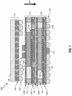
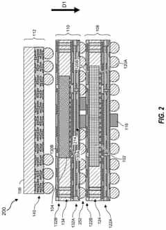
3D chiplet integration using fan-out wafer-level packaging
PatentPendingUS20240274587A1
Innovation
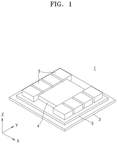
- The use of fan-out wafer-level packaging and three-dimensional packaging techniques for combining semiconductor chips and embedded memory in configurations such as face-to-back, back-to-back, and face-to-face orientations, enabling direct connections between chiplets and reducing assembly package sizes and manufacturing complexity.
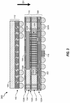
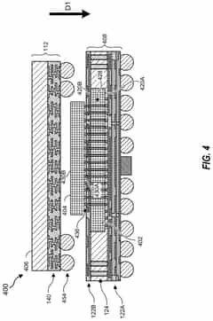
Semiconductor device
PatentPendingUS20250293165A1
Innovation
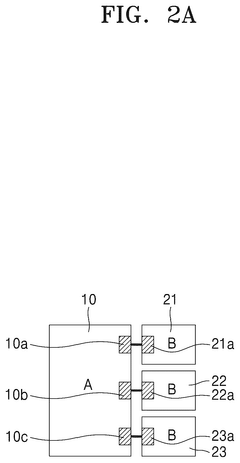
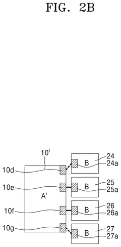
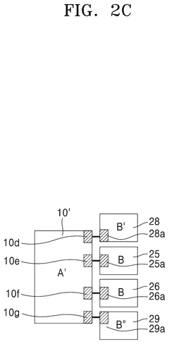
- A semiconductor device with configurable chiplet dies and an interposer, featuring a die-to-die interface with adjustable modules and a selection circuit that allows for variable alignment of connection modules, enabling efficient inter-chiplet communication without the need for new chiplet designs.
Standardization Efforts in Chiplet Interfaces
The standardization of chiplet interfaces represents a critical foundation for the broader adoption and evolution of chiplet technology in the semiconductor industry. Currently, several industry consortia and organizations are actively developing standards to address interoperability challenges between chiplets from different vendors.
The Universal Chiplet Interconnect Express (UCIe) consortium, formed in 2022, has emerged as a leading standardization effort. UCIe focuses on establishing die-to-die interconnect standards that enable chiplets from different manufacturers to work seamlessly together. The standard defines both physical and protocol layers, covering aspects such as electrical specifications, physical design, and communication protocols. Major industry players including Intel, AMD, Arm, TSMC, and Samsung have joined this initiative, signaling strong industry commitment.
Another significant standardization effort is the Open Compute Project's (OCP) Chiplet Design Exchange (CDX) framework. CDX aims to create standardized models and interfaces for chiplet-based designs, facilitating easier integration and verification processes. This framework addresses not only electrical interfaces but also thermal, mechanical, and testing considerations that are essential for successful chiplet integration.
JEDEC, a well-established semiconductor engineering standardization organization, has also entered the chiplet standardization arena with its JC70 committee focusing on wide I/O interfaces and chiplet standardization. Their work complements other efforts by addressing memory integration aspects, which are particularly crucial for high-performance computing applications.
The Advanced Interface Bus (AIB) developed by Intel represents another important standard that has gained traction. AIB provides a die-to-die parallel interface protocol that enables high-bandwidth, low-latency communication between chiplets. Intel has made AIB available through open licensing, encouraging wider adoption across the industry.
These standardization efforts face several challenges, including balancing technical requirements with commercial interests, ensuring backward compatibility, and addressing the diverse needs of different application domains. The evolution of these standards will significantly impact the chiplet ecosystem's development trajectory.
The convergence toward unified standards is gradually taking shape, though complete standardization remains a work in progress. Industry analysts predict that standardized chiplet interfaces could reduce design costs by up to 30% and accelerate time-to-market by 40% for complex semiconductor products, highlighting the economic importance of these standardization efforts beyond their technical significance.
Thermal Management Solutions for Chiplet Designs
Thermal management has emerged as a critical challenge in chiplet-based semiconductor designs. As chiplets enable higher integration densities and performance levels, they also generate significant heat concentrations that must be effectively dissipated to maintain reliability and performance. Current thermal management solutions for chiplet designs can be categorized into several approaches, each addressing different aspects of the thermal challenge.
Direct liquid cooling technologies have gained prominence, with microchannel cooling solutions integrated directly into the interposer or substrate. These systems circulate coolant through microscopic channels positioned close to heat-generating components, enabling more efficient heat transfer compared to traditional air cooling methods. Some advanced implementations incorporate two-phase cooling, where the liquid-to-vapor phase change provides enhanced thermal absorption capacity.
Advanced thermal interface materials (TIMs) represent another crucial development area. Novel composite materials incorporating graphene, carbon nanotubes, and metallic nanoparticles have demonstrated thermal conductivities 2-3 times higher than conventional TIMs, significantly reducing thermal resistance between chiplets and heat spreaders. These materials are engineered to maintain performance over thousands of thermal cycles, addressing reliability concerns in heterogeneous integration scenarios.
Architectural thermal optimization techniques have also evolved specifically for chiplet designs. Dynamic thermal management systems now incorporate chiplet-aware algorithms that can selectively throttle specific chiplets based on workload distribution and thermal conditions. This granular approach preserves overall system performance while preventing localized hotspots. Additionally, thermal-aware floorplanning tools now consider heat distribution patterns when determining optimal chiplet placement within a package.
3D integration thermal solutions address the unique challenges of vertically stacked chiplets. Through-silicon vias (TSVs) are increasingly being designed to serve dual purposes as both electrical interconnects and thermal conduits. Some advanced designs incorporate dedicated thermal TSVs filled with high-conductivity materials to create vertical heat evacuation pathways. Complementing this approach, integrated micro heat pipes embedded within the interposer provide lateral heat spreading capabilities.
Emerging technologies include phase-change materials embedded within the package that absorb heat during high-load operations and release it during idle periods, effectively dampening thermal transients. Research into diamond-based heat spreaders shows promise, with synthetic diamond films demonstrating thermal conductivity values exceeding 1500 W/mK, approximately four times that of copper.
Unlock deeper insights with Patsnap Eureka Quick Research — get a full tech report to explore trends and direct your research. Try now!
Generate Your Research Report Instantly with AI Agent
Supercharge your innovation with Patsnap Eureka AI Agent Platform!