

Analyzing Global Standards for Semiconductor Chiplet Integration
OCT 15, 20259 MIN READ
Generate Your Research Report Instantly with AI Agent
Patsnap Eureka helps you evaluate technical feasibility & market potential.
Chiplet Integration Standards Background and Objectives
The evolution of semiconductor technology has historically followed Moore's Law, with continuous miniaturization of transistors on a single chip. However, as physical limitations increasingly challenge further scaling, the industry has pivoted toward chiplet architecture as a promising alternative. Chiplet technology involves disaggregating traditional monolithic system-on-chip designs into smaller functional blocks that can be manufactured separately and then integrated into a complete system. This approach emerged around 2015-2017 when leading semiconductor companies began exploring modular chip designs to overcome yield, cost, and performance challenges.
The primary objective of chiplet integration standards is to establish a unified framework that enables heterogeneous integration of semiconductor components from different vendors. These standards aim to define common interfaces, protocols, and physical specifications that facilitate seamless communication between chiplets, regardless of their manufacturing origin or process technology. By creating an ecosystem of interoperable chiplets, the industry seeks to accelerate innovation, reduce development costs, and enhance system performance beyond what traditional monolithic designs can achieve.
The technical evolution trajectory shows a clear progression from proprietary chiplet implementations toward open standards. Initially, companies like AMD with its Infinity Fabric and Intel with EMIB (Embedded Multi-die Interconnect Bridge) developed in-house solutions. However, the industry recognized that proprietary approaches limited the potential of chiplet technology, leading to collaborative standardization efforts such as UCIe (Universal Chiplet Interconnect Express) in 2022, which brought together competitors including Intel, AMD, Arm, TSMC, and Samsung.
Current standardization efforts focus on several critical aspects: die-to-die interfaces that define electrical and physical connections between chiplets; communication protocols that ensure efficient data transfer; power management specifications; thermal considerations; and testing methodologies. The ultimate goal is to create a "chiplet marketplace" where semiconductor components from various manufacturers can be integrated as easily as plugging together standardized electronic components on a printed circuit board.
The development of these standards represents a fundamental shift in semiconductor design philosophy, moving from vertical integration toward horizontal specialization. This transition enables companies to focus on their core competencies while leveraging the innovations of others through standardized interfaces. As chiplet technology matures, these standards will play a crucial role in addressing the increasing complexity and cost of advanced node semiconductor manufacturing, potentially democratizing access to cutting-edge system capabilities across the industry.
Market Demand Analysis for Chiplet Technology
The chiplet technology market is experiencing unprecedented growth driven by the increasing demand for advanced computing solutions across multiple industries. As traditional monolithic chip designs reach their physical and economic limits, chiplet-based architectures have emerged as a compelling alternative, offering improved yield, cost efficiency, and performance scalability. Market research indicates that the global chiplet market is projected to grow at a compound annual growth rate of 38% from 2023 to 2030, reaching approximately 57 billion USD by the end of the forecast period.
The primary market drivers for chiplet technology include the exponential growth in data center infrastructure, artificial intelligence applications, and high-performance computing systems. Cloud service providers are particularly interested in chiplet solutions as they enable more efficient server architectures with customizable computing resources. Additionally, the automotive industry is increasingly adopting advanced semiconductor solutions for autonomous driving systems, creating another significant market segment for chiplet technology.
Consumer electronics manufacturers are also exploring chiplet integration to deliver more powerful mobile devices while maintaining energy efficiency. This sector represents a substantial volume opportunity, though with different performance and cost requirements compared to data center applications. The diversification of market demand across these segments highlights the versatility of chiplet technology and its potential to address various computing needs.
From a geographical perspective, North America currently leads the chiplet market due to the concentration of major semiconductor companies and technology innovators. However, Asia-Pacific is expected to witness the fastest growth rate, driven by substantial investments in semiconductor manufacturing infrastructure in countries like Taiwan, South Korea, and China. The European market is also showing increased interest, particularly in automotive and industrial applications.
Supply chain considerations are becoming increasingly critical in market demand analysis. The geopolitical tensions and recent supply chain disruptions have accelerated interest in chiplet technology as it potentially allows for more distributed manufacturing processes and reduced dependency on single-source components. This aspect is particularly appealing to governments and corporations seeking to enhance supply chain resilience.
The market demand for standardized chiplet interfaces is particularly strong, as evidenced by industry consortiums like Universal Chiplet Interconnect Express (UCIe) gaining significant traction. Customers across sectors are expressing preference for solutions that adhere to open standards, which facilitate multi-vendor integration and reduce the risk of vendor lock-in. This standardization trend is expected to accelerate market adoption and expand the ecosystem of chiplet-compatible products.
Global Chiplet Standards Landscape and Challenges
The global chiplet integration landscape is characterized by a complex ecosystem of competing and complementary standards, reflecting the industry's transition from monolithic system-on-chip designs to more modular approaches. Currently, several major standards are vying for dominance, including Universal Chiplet Interconnect Express (UCIe), Advanced Interface Bus (AIB), Bunch of Wires (BoW), High Bandwidth Memory (HBM), and Open Domain-Specific Architecture (ODSA).
UCIe, backed by industry giants including Intel, AMD, Arm, TSMC, and Samsung, has emerged as a frontrunner in establishing a comprehensive die-to-die interconnect standard. The consortium's approach encompasses both physical and protocol layers, providing a complete framework for chiplet integration across different manufacturers. This standard's strength lies in its broad industry support and comprehensive scope.
Competing with UCIe is AIB, developed by Intel and now in its third generation. AIB offers high bandwidth density and power efficiency but remains somewhat proprietary despite being available through open licensing. Similarly, BoW, developed by the ODSA, presents a simpler alternative focused on cost-effectiveness and ease of implementation, particularly appealing for less demanding applications.
The fragmentation of standards presents significant challenges for the semiconductor industry. Interoperability issues arise when attempting to integrate chiplets designed to different standards, creating technical barriers that impede the vision of a truly open chiplet ecosystem. This fragmentation also increases design complexity and potentially raises costs, as manufacturers must support multiple interface protocols.
Geopolitical tensions further complicate the standards landscape, with different regions potentially favoring standards developed by their domestic champions. The US-China technology competition, in particular, risks creating separate ecosystems with limited compatibility, potentially fragmenting the global supply chain.
Intellectual property considerations present another layer of complexity, as standards may incorporate patented technologies requiring licensing agreements. This can create barriers to adoption, especially for smaller players with limited resources for negotiating complex IP arrangements.
The industry faces a critical challenge in balancing innovation with standardization. While standardization promotes interoperability and market growth, premature convergence on suboptimal standards could stifle innovation. Finding the right balance requires collaborative industry efforts and potentially regulatory guidance.
Moving forward, the industry must address these challenges through increased collaboration, potentially through neutral industry consortia that can facilitate consensus-building across competing interests. Government policies supporting open standards could also play a crucial role in preventing market fragmentation along geopolitical lines.
Current Chiplet Integration Methodologies
01 Universal Chiplet Interconnect Express (UCIe) Standards
UCIe is an open industry standard for chiplet integration that defines the physical layer, protocol stack, and software interfaces for die-to-die interconnection. This standard enables interoperability between chiplets from different vendors, allowing for more flexible and cost-effective semiconductor designs. UCIe supports high-bandwidth, low-latency connections between chiplets while maintaining power efficiency, which is crucial for advanced computing applications.- Universal Chiplet Interconnect Standards: Universal Chiplet Interconnect Express (UCIe) and other standardized interfaces enable seamless integration of chiplets from different manufacturers. These standards define electrical specifications, physical layer protocols, and communication interfaces to ensure interoperability between heterogeneous chiplets. Standardized interconnects reduce design complexity and enable a modular approach to semiconductor system design, allowing companies to mix and match chiplets from various vendors.
- Advanced Packaging Technologies for Chiplet Integration: Various advanced packaging technologies support chiplet integration, including 2.5D and 3D integration approaches. These technologies utilize silicon interposers, through-silicon vias (TSVs), and micro-bumps to connect multiple chiplets within a single package. Advanced packaging solutions address thermal management challenges, signal integrity issues, and power delivery concerns that arise when integrating multiple chiplets in close proximity.
- Die-to-Die Communication Protocols: Specialized communication protocols optimize data transfer between chiplets while minimizing power consumption and latency. These protocols include high-bandwidth, low-power interfaces specifically designed for die-to-die communication within a package. Standardized communication protocols ensure reliable data exchange between chiplets and support various bandwidth requirements for different applications, from high-performance computing to mobile devices.
- Chiplet Design and Verification Methodologies: Standardized design and verification methodologies ensure chiplet compatibility and system-level functionality. These methodologies include design-for-test approaches, boundary scan techniques, and built-in self-test capabilities specific to chiplet-based systems. Standardized verification processes validate chiplet interfaces, timing requirements, and electrical characteristics to ensure proper integration into multi-chiplet systems.
- Chiplet-based System-on-Chip Integration: Integration frameworks for combining chiplets into complete system-on-chip solutions address system-level concerns including power management, thermal distribution, and signal integrity. These frameworks provide standardized approaches for chiplet placement, routing, and integration with common IP blocks. System-level integration standards ensure optimal performance while maintaining the modularity and flexibility benefits of chiplet-based design.
02 Advanced Packaging Technologies for Chiplet Integration
Advanced packaging technologies are essential for effective chiplet integration, including 2.5D and 3D integration approaches. These technologies involve the use of interposers, through-silicon vias (TSVs), and micro-bumps to connect multiple chiplets within a single package. Such packaging methods enable higher bandwidth, reduced latency, and improved thermal management compared to traditional monolithic designs, while allowing for the combination of chiplets manufactured using different process nodes.Expand Specific Solutions03 Die-to-Die Interface Protocols and Communication Standards
Standardized die-to-die interface protocols are critical for ensuring reliable communication between chiplets. These protocols define signal integrity requirements, clock synchronization methods, and error correction mechanisms. They include specifications for physical layer connections, data encoding schemes, and flow control mechanisms. Standardized interfaces reduce design complexity and enable chiplets from different manufacturers to work together seamlessly, accelerating time-to-market for heterogeneous integrated systems.Expand Specific Solutions04 Thermal Management and Power Distribution for Chiplet Systems
Effective thermal management and power distribution are crucial challenges in chiplet-based designs. Standards address the need for uniform power delivery across multiple chiplets and efficient heat dissipation from densely packed components. These include specifications for thermal interface materials, power delivery networks, and cooling solutions tailored for heterogeneous integration. Standardized approaches help manage thermal hotspots and ensure reliable operation under varying workloads while maintaining system performance.Expand Specific Solutions05 Testing and Validation Standards for Chiplet-Based Systems
Testing and validation standards for chiplet-based systems define methodologies for verifying the functionality and reliability of integrated chiplets. These standards include specifications for known-good-die testing, interconnect validation, and system-level performance verification. They address unique challenges in testing disaggregated designs, such as interface compliance testing and inter-chiplet communication validation. Standardized testing approaches help ensure quality and reliability while reducing validation costs and time-to-market for chiplet-based products.Expand Specific Solutions
Key Industry Players in Chiplet Standardization
The semiconductor chiplet integration market is currently in a growth phase, with increasing adoption driven by the need for advanced packaging solutions to overcome traditional scaling limitations. The global market size is expanding rapidly, projected to reach significant value as chiplet technology becomes essential for next-generation computing systems. From a technical maturity perspective, industry leaders like TSMC, Intel, and Samsung Electronics are at the forefront, having developed advanced chiplet integration technologies and standards. Companies including NXP, Renesas, and SK hynix are actively investing in this space, while newer entrants like Chipletz are introducing innovative solutions. Academic institutions such as Zhejiang University and Harbin Institute of Technology are contributing research advancements. The competitive landscape is characterized by collaboration on universal standards while companies simultaneously develop proprietary technologies to maintain competitive advantages.
Taiwan Semiconductor Manufacturing Co., Ltd.
Technical Solution: TSMC has pioneered advanced chiplet integration through their CoWoS (Chip-on-Wafer-on-Substrate) and InFO (Integrated Fan-Out) packaging technologies. Their CoWoS platform enables heterogeneous integration of multiple chiplets using silicon interposers with high-density interconnects, supporting bandwidth up to 8 TB/s between chiplets. TSMC has also developed their 3DFabric architecture which combines frontend and backend technologies to create a comprehensive 3D silicon stacking and advanced packaging platform. Their LIPINCON (Low-voltage-In-Package-INterCONnect) technology provides ultra-high bandwidth, low power consumption chip-to-chip interconnects specifically designed for chiplet architectures. TSMC actively participates in the Universal Chiplet Interconnect Express (UCIe) consortium to establish open standards for die-to-die interconnects.
Strengths: Industry-leading process nodes (down to 3nm) providing superior integration capabilities; extensive IP ecosystem; high-volume manufacturing expertise. Weaknesses: Proprietary technologies may limit interoperability with other vendors' chiplets; high implementation costs for smaller companies; capacity constraints during high demand periods.
Samsung Electronics Co., Ltd.
Technical Solution: Samsung has developed their I-Cube (Interposer-Cube) technology for chiplet integration, which uses silicon interposers to connect multiple dies with high-bandwidth memory (HBM). Their advanced X-Cube technology employs TSVs (Through-Silicon Vias) to enable true 3D stacking of heterogeneous chiplets, achieving significant form factor reductions and performance improvements. Samsung's FOPLP (Fan-Out Panel Level Packaging) technology extends chiplet integration capabilities to panel-sized substrates, improving manufacturing efficiency and reducing costs. They've also introduced their own die-to-die (D2D) interface technology that achieves data rates up to 2.5 GT/s while maintaining low power consumption of 0.5pJ/bit. Samsung actively participates in the UCIe consortium and has announced plans to implement UCIe-compliant interfaces in their future chiplet designs to ensure interoperability with other vendors' components.
Strengths: Vertical integration from design to manufacturing; extensive memory technology expertise that complements chiplet integration; advanced process nodes available in-house. Weaknesses: Less established ecosystem for third-party chiplet integration compared to TSMC; historically more focused on memory than logic integration.
Critical Patents and Technical Literature Review
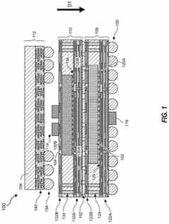
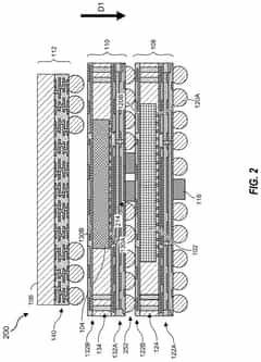
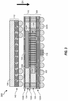
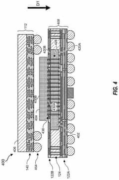
3D chiplet integration using fan-out wafer-level packaging
PatentPendingUS20240274587A1
Innovation
- The use of fan-out wafer-level packaging and three-dimensional packaging techniques for combining semiconductor chips and embedded memory in configurations such as face-to-back, back-to-back, and face-to-face orientations, enabling direct connections between chiplets and reducing assembly package sizes and manufacturing complexity.
Data transmission system suitable for aerospace chiplet interconnection protocol
PatentPendingCN117331881A
Innovation
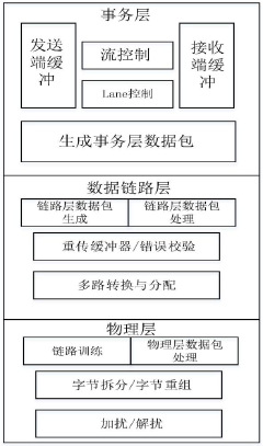
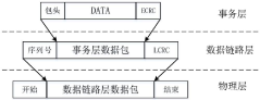
- 设计一种适用于宇航chiplet互联协议的数据传输系统,包括事务层、数据链路层和物理层,通过仲裁器实现高速数据传输,使用CRC校验和纠错机制增强可靠性,转换多比特并行数据为串行数据,通过串行接口进行高速传输。
Supply Chain Implications of Chiplet Standardization
The standardization of chiplet interfaces is fundamentally reshaping semiconductor supply chains, creating both opportunities and challenges for industry participants. As chiplet technology enables disaggregation of system-on-chip designs into smaller functional blocks, it introduces new dynamics in how semiconductor components are sourced, manufactured, and integrated.
The emergence of universal standards like Universal Chiplet Interconnect Express (UCIe) is democratizing access to advanced packaging technologies. This standardization allows smaller design houses to focus on specialized chiplets without needing to develop complete SoC solutions, potentially disrupting traditional semiconductor value chains dominated by integrated device manufacturers (IDMs).
From a manufacturing perspective, chiplet standardization enables more distributed production models. Different chiplets within a single package can be manufactured by various foundries using their optimal process nodes. This flexibility creates resilience against regional supply disruptions and geopolitical tensions that have plagued monolithic chip production in recent years.
The testing and validation ecosystem is also evolving in response to chiplet standardization. New specialized service providers are emerging to handle the complex testing requirements of multi-chiplet designs, creating additional nodes in the supply chain. These specialized testing services represent a growing market segment as chiplet adoption increases across computing sectors.
Inventory management strategies are being reconsidered as standardized chiplets potentially enable more modular approaches to semiconductor procurement. Companies can maintain inventories of common chiplets that can be rapidly integrated into various end products, potentially reducing lead times and improving responsiveness to market demands.
Geographically, chiplet standardization may accelerate the regionalization of semiconductor supply chains. As advanced packaging becomes a critical differentiator, countries are investing heavily in packaging capabilities to complement fabrication facilities. This trend could reshape the global distribution of semiconductor manufacturing value, with regions specializing in different aspects of the chiplet ecosystem.
The intellectual property landscape is also transforming, with new licensing models emerging for chiplet designs and interface technologies. This evolution creates opportunities for IP-focused companies to participate in the chiplet economy without significant manufacturing investments, further diversifying the supply chain.
Geopolitical Factors Affecting Semiconductor Standards
The geopolitical landscape has become increasingly influential in shaping semiconductor chiplet integration standards globally. The technology sector, once driven primarily by technical considerations and market forces, now operates within a complex web of national security interests, trade policies, and technological sovereignty concerns. The United States, China, and the European Union have emerged as the primary actors in this arena, each pursuing distinct approaches to semiconductor standardization that align with their strategic objectives.
The US-China technological rivalry has significantly impacted the development of global chiplet standards. Following restrictions on semiconductor technology exports to China, parallel standardization efforts have emerged. The United States has leveraged its technological leadership through organizations like CHIPS Alliance and Open Compute Project to promote standards that maintain Western technological advantages. Meanwhile, China has accelerated domestic semiconductor capabilities through initiatives like "Made in China 2025" and established alternative standardization bodies such as the China Semiconductor Industry Association (CSIA).
Regional blocs are forming around semiconductor standards, with nations increasingly aligning with either US-led or China-led ecosystems. This bifurcation threatens the historically global nature of semiconductor standards and raises concerns about interoperability challenges. The European Union has positioned itself as a potential bridge between these competing systems while pursuing "technological sovereignty" through initiatives like the European Chips Act.
National security considerations have become central to semiconductor standardization decisions. Governments increasingly view control over semiconductor technology as essential to military capabilities, critical infrastructure protection, and economic security. This has led to the implementation of investment screening mechanisms, export controls, and domestic manufacturing incentives that directly influence which standards gain prominence.
Supply chain resilience has emerged as a key factor in standards development following pandemic-related disruptions and geopolitical tensions. Nations are prioritizing standards that enable diversified manufacturing capabilities and reduce dependencies on potentially hostile countries. This has accelerated interest in modular chiplet designs that allow for more flexible manufacturing arrangements across geopolitically diverse locations.
International standards organizations like IEEE and ISO face mounting pressure to navigate these geopolitical tensions. Their traditional consensus-based approach is challenged by competing national interests, raising questions about the future viability of truly global semiconductor standards. Some organizations have established specialized working groups focused on balancing innovation with security considerations in chiplet integration standards.
Unlock deeper insights with Patsnap Eureka Quick Research — get a full tech report to explore trends and direct your research. Try now!
Generate Your Research Report Instantly with AI Agent
Supercharge your innovation with Patsnap Eureka AI Agent Platform!